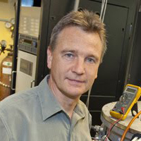
Speaker:Prof.André Anders,Lawrence Berkeley National Laboratory, Berkeley, California
Sponsor:Prof.QIN Hua
Time: 10:00a.m.Tuesday,September 2nd
Place:A722,SINANO
Abstract:
Thin films have microstructures that are distinctly different from the structure of bulk materials. Film microstructure is greatly influenced by the method of film deposition and deposition conditions. This was recognized in the 1960s by Movchan and Demchishin for films made by evaporation [1] , and described later by Thornton for sputter-deposited films [2]. The two major parameter “knobs” were the substrate temperature and sputtering gas pressure. With the advent of plasma-assistance, many more parameter “knobs” became available due to the presence of ions and electrons, which contribute to the film growth process through kinetic and potential energies. This can be illustrated in a generalized Thornton structure zone diagram [3]. In particular, substrate biasing techniques can affect interface intermixing, film density, compressive stress, and crystal grain size, and all the film properties that are derived from the film microstructure.
[1] B.A. Movchan, A.V. Demchishin, Fizika Metallov i Metallovedenie (Physics of Metals and Metallography) 28 (1969) 653.
[2] J.A. Thornton, J. Vac. Sci. Technol. A 4 (1986) 3059.
[3] A. Anders, Thin Solid Films 518 (2010) 4087.
Bio:
Dr. Anders earned his Ph.D. in physics at Humboldt University Berlin, Germany in 1987. Following appointments as Staff Scientist at the Central Institute for Electron Physics (The Academy of Sciences) in (East) Berlin, Germany, and the Max Planck Institute for Plasma Physics in Garching, Germany, Dr. Anders joined Lawrence Berkeley National Laboratory (LBNL) in Berkeley, California, in 1992. Currently holding the prestigious position of Senior Scientist and Leader of the Plasma Applications Group at LBNL, Dr. Anders’ research focuses on plasma physics and materials science, and his research interests include coatings and thin film synthesis, high power impulse magnetron sputtering, cathodic vacuum arc plasma and ion sources, gas plasma sources, ion implantation, and plasma immersion ion implantation, transparent conducting oxides, and electrochromic materials. Dr. Anders has published three books, authored or co-authored more than 300 articles in peer-reviewed publications and holds 16 patents. He is recognized by election to Fellow of four scientific societies (APS, AVS, IEEE, IoP) and through numerous awards, including the Walter Dyke Award, the highest award of the International Symposia on Electrical Discharges and Insulation in Vacuum (2014), Mentor Award of the Society of Vacuum Coaters (2011), IEEE Merit Award of the IEEE Nuclear and Plasma Sciences Society (2010), and the Chatterton Award (1994). In 2016 he received the Nathaniel H. Sugerman Memorial Award, the highest award of the Society of Vacuum Coaters (SVC). Dr. Anders has served as Associate Editor of Journal of Applied Physics from 2009 to 2014, and was appointed Editor-in-Chief in 2014.
Professional Activities and Awards: Fellow of the American Physical Society, Fellow of the American Vacuum Society, Fellow of the Fellow of the Institute of Electrical and Electronics Engineers, and Fellow of the Institute of Physics. Prof. Anders has been recognized through numerous awards, including the Walter Dyke Award, the highest award of the International Symposia of Electrical Discharges and Insulation in Vacuum (2014), Mentor Award of the Society of Vacuum Coaters (2011), IEEE Merit Award of the IEEE Nuclear and Plasma Sciences Society (2010), and the Chatterton Award (1994).
downloadFile
