On March 28th, 2019, Dr. Atsushi Nishikawa from ALLOS Semiconductors GmbH visited Key Laboratory of Nano-devices and Applications, Chinese Academy of Sciences (CAS), and Vacuum Interconnected Nano-X Research Facility at Suzhou Institute of Nano-Tech and Nano-Bionics (SINANO), CAS.
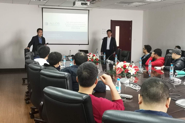
Dr. Atsushi Nishikawa also gave an exciting scientific report with the title of "High crystal quality GaN-on-Si to achieve excellent isolation and dynamic performance without carbon doping" on the morning of March 28th. In this talk, he introduced the development of GaN-on-Si growth technologies with epitaxial lateral overgrowth and interlayers for crystal quality improvement for high isolation without carbon doping and precise strain-engineering. As a result, he has successfully obtained 7 μm thick and high crystal quality GaN layer on Si substrate. GaN-on-Si HEMTs show vertical and lateral grounded leakage current as low as 0.003 μA/mm2 and 0.007 μA/mm at 600 V, respectively. Physical breakdown does not occur up to 1200 V. The critical electric field derived from lateral floating current-voltage measurements is as high as 1.7 MV/cm, which is much higher than typically reported values (< 1.0 MV/cm).
Dr. Atsushi Nishikawa is Chief Technology Officer of ALLOS Semiconductors GmbH, an international IP licensing and developing company for GaN-on-Si patents and technology. Nishikawa has more than 15 years’ experience in MOCVD growth of III-nitride. Prior to co-founding ALLOS he was head of epitaxy at GaN-on-Si pioneer AZZURRO Semiconductors and worked in GaN-related research at NTT Basic Research Labs and Osaka University. At ALLOS he continues to head the advancement of the technology as well as the transfer of ALLOS’ GaN-on-Si technology to its customers’ reactors.
downloadFile