Printable electronics has become the flourishing development technology in the last 5 years, and it is regarded as hot topics of the interdisciplinary and frontier researches, which has attracted more and more attention in recent years due to their potential applications in large-area and flexible electronic systems. According to IDTechEx’s market research report, by 2022 the printed electronics market will be worth $63 billion, containing 45% printed and 33% on flexible substrates. Development of high-performance printable electronic inks, such as printable semiconducting ink, dielectric inks and conductor inks, plays a key role in printable electronics. A good semiconducting ink should generally have high carrier mobility, chemical stability, and the functional materials can be solution-processed at low temperature. Single-walled carbon nanotubes (SWCNTs) are one of the most promising materials for printable inks because SWCNTs have excellent physical, chemical, mechanical properties, chemical stability and high mobility (mobility of individual semiconducting SWCNT is of ~104 cm2 V-1?s-1), and can be easily dispersed well in several organic solvents and aqueous solution with the aid of sonication.
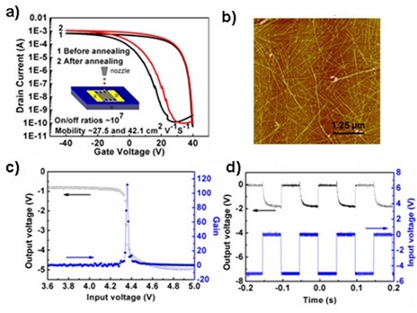
Printable Electronics Research Center, Suzhou Institute of Nano-tech and Nano-biotics, Chinese Academy of Science, have developed several methods to separate sc-SWCNTs from commercial SWCNTs, such as chemical selective reaction, polymer wrapping and so on, and fabricated high-performance printable TFTs (mobility and on/off ratio up to 40 cm2/Vs and 107, respectively), all-printed flexible transistors and high-performance inverters. These works have demonstrated that printable SWCNT TFTs have the potential in OLED and LED displays in the future.
The relative works were published in Nanoscale (2013, 5, 4156-4161), JPCC (2013, DOI: 10.1021/jp4055022 and 2011, 115, 6975-6979), JMC (2012, 22, 2051-2056 and 2012, 22, 20747–20753), Sci China Chem (2011, 54: 1484-1490.), and 4 China Patents (No201210102957.8, 201210098673.6, 201210563804.3 and 201310077635.7)were applied.
This work was supported by the Knowledge Innovation Programme of the Chinese Academy of Sciences (KJCX2-EW-M02), Natural Science Foundation of China (91123034, 61102046), and Basic Research Programme of Jiangsu Province (BK2011364 ).

Figure 1 a) transfer curves of printed TFTs based on sorted SWCNTs before and after annealing (Vds=-2 V), b) typical AFM imaging of SWCNTs in the channeal; c) input-output and gain characteristics of an inverter at Vdd= -5 V. The value of Gain is 112, and d) the input and output characteristic of a SWCNT inverter at 10 Hz.(Image by SINANO)
downloadFile
