Solar energy is one of the most important renewable energy sources. Thin film photovoltaic devices have become the focus of R&D for the next generation solar energy harvesting technology due to their low cost, high efficiency, facile fabrication, and mechanical flexibility.
Energy band alignment in photovoltaic device is critically important because it largely governs elementary photovoltaic processes, such as the separation, transport, recombination and collection of charge carriers, which, in turn, determine the power conversion performance of the device. However, it is still an out-standing challenge in the PV field to characterize the energy band alignment, especially under operando conditions.
Recently, Prof. Liwei Chen’s research group in the Suzhou Institute of Nano-Tech and Nano-Bionics (SINANO), Chinese Academy of Sciences (CAS), has developed a method for quantitative operando visualization of the energy band alignment in thin film photovoltaic devices.
The developed method involves the exposure of thin-film PV device cross section by ion-beam milling, and then the imaging of the surface potential depth profile using scanning Kelvin probe microscopy (SKPM) (Figure 1a-c), which equals the vacuum level profile upon multiplication of the absolute charge of an electron. Quantitative investigations reveal that the SKPM tip-size and cantilever beam crosstalk induced convolution effect results in systematic smoothing and averaging of the energy band depth profile in the measurement. Nevertheless, a bias compensation method is developed to obtain quantitatively accurate measurements of internal potential difference parameters, such as open-circuit voltage, built-in potential and electrode potential difference (Figure 1d). This work was published in Nature Communications 6:7745 (2015).
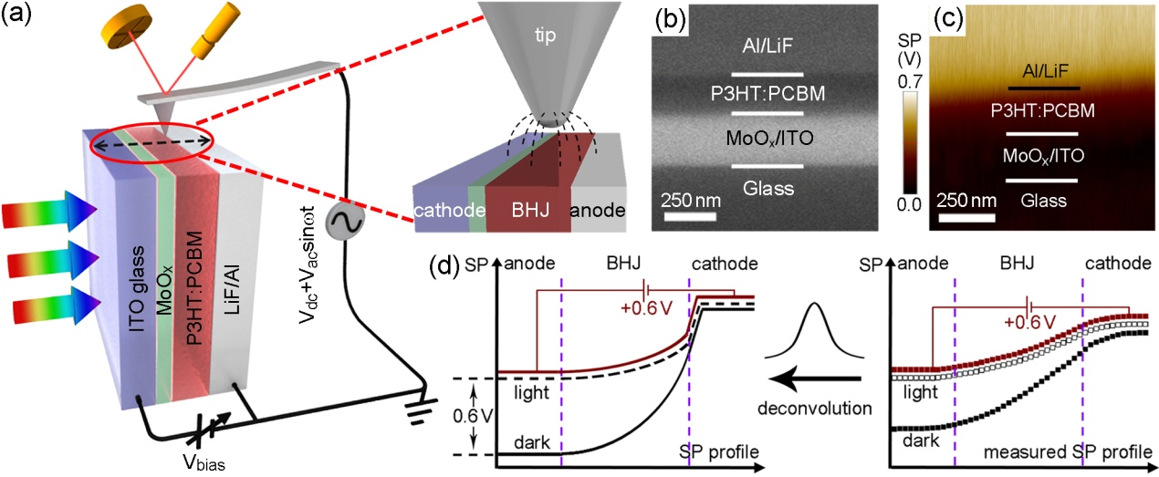
Figure 1. (a) A schematic illustration of cross-sectional SKPM imaging on operando OPV devices. (b) SEM image of an OPV device cross-section. (c) Surface potential image of an OPV device cross-section in dark and open-circuit. (d) illustrated principle of the bias compensation method for quantitative measurement.(Image by CHEN Liwei's group)
This mechanistic research was an integrated part of the thin-film solar energy program at SINANO. Partially supported by the Collaborative Innovation Center of Suzhou Nano Science and Technology, the solar energy research program at the Collaborative Energy Nanotechnology Center at SINANO, which consists of researchers from the Chen group, Profs. Changqi Ma and Shulong Lu’s groups, focuses on practical thin-film solar technologies based on organic semiconductor, inorganic semiconductor, and organometallic perovskite materials. Together with research divisions of the Printing Electronics, Nano Devices, and the i-Lab, the solar energy team has reported the highest power conversion efficiency organic PV device with active cell area > 1 cm2 (5.85 % efficiency at 1.2 cm2 device area, Figure 2a-b), which features a Ag-nano grid based flexible and transparent hybrid electrode without ITO (Suzhou NanoGrid Technology Ltd.). The team also puts an emphasis on practical manufacturing techniques as well as device stability testing (Figure 2c) and encapsulation techniques. Researches on high-efficiency large-area thin-film solar cells based on perovskite and III-V semiconducting materials are currently underway. [Nano Energy 10, 259 (2014); Solar Energy Materials & Solar Cells 113, 85 (2013); Solar Energy Materials & Solar Cells, 143, 354 (2015)].
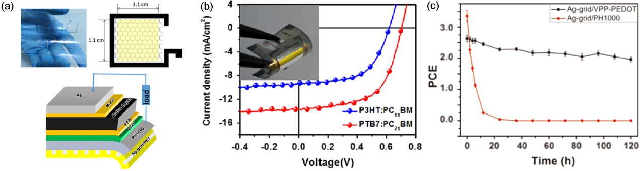
Figure 2. (a) Photograph and schematic illustration of the Ag-nano grid hybrid electrode based large-area OPV devices. (b) J-V performance of the large-area OPV devices. (c) Ambient stability test of large-area OPV devices with different electrodes.(Image by CHEN Liwei's group)
This series of research are funded by the National Natural Science Foundation of China, Jiangsu Provincial Natural Science Foundation, Collaborative Innovation Center of Suzhou Nano Science and Technology, and Suzhou Institute of Nanotech and Nanobionics, Chinese Academy of Sciences.
downloadFile