Recently, a research team led by Prof. SUN Qian in Key Laboratory of Nano-devices and Applications, Suzhou Institute of Nano-Tech and Nano-Bionics (SINANO), Chinese Academy of Sciences has reported the realization of room-temperature electrically injected AlGaN-based near ultraviolet (NUV) laser grown on Si.
AlGaN-based ultraviolet (UV) laser diodes (LDs) have attracted intense research interest in the last few years due to their great potential application. They may provide alternative solutions to conventional gas and solid-state UV lasers which are large, heavy, inefficient, and inflexible in emission wavelength.
Today most of the AlGaN-based UV LDs are epitaxially grown on costly free-standing GaN substrates or expensive small-size bulk AlN substrates. By replacing these small-size expensive substrates with large-diameter cost-effective Si substrates, the cost of AlGaN-based UV LDs can be cut down to the level of light-emitting diode cost.
Several other research groups attempted to grow III-nitride materials on Si and only achieved optically pumped lasing. Recently, we have demonstrated the world’s first room-temperature electrically injected InGaN-based visible LD grown on Si in Nature Phonics entitled “Room-temperature continuous-wave electrically injected InGaN-based laser directly grown on Si”.
To push the lasing wavelength from visible to UV, realization of AlGaN-based NUV LDs grown on Si needs to overcome several critical issues, which are even more challenging than that of InGaN-based visible LDs on Si. Compared with visible quantum wells (QWs), the internal quantum efficiency of NUV QWs is much more sensitive to the threading dislocation (TD) density. However, direct growth of AlGaN on Si substrate encounters a very high TD density because of the large lattice mismatch.
Furthermore, a huge misfit in coefficient of thermal expansion (CTE) between AlGaN and Si substrate usually induces a large tensile stress in the epitaxial film, and hence limits the maximum thickness of crack-free epitaxial film directly grown on Si.
In AlGaN-based UV LDs, AlGaN-based cladding layers (CLs) with a relatively high Al content (~10%) are usually utilized to enhance the optical confinement of the active region. To avoid the formation of micro-cracks, thick AlGaN template is often used to replace the conventional GaN template and hence reduce the tensile stress.
The thick AlGaN-based optical CLs and the GaN-based waveguide layers, together with the NUV QWs and the contact layers, often add up to a total thickness of 6-7 μm. However, it is quite challenging to grow crack-free high-quality AlGaN-containing 6-7 μm thick film on Si substrate.
In this work, an Al-composition step down-graded AlN/AlGaN multilayer buffer was carefully engineered to circumvent the lattice mismatch and the CTE misfit for the epitaxial growth of high-quality Si-doped n-type AlGaN thick template on Si substrate. On top of the AlGaN template, an AlGaN-based NUV laser structure was grown. After device fabrication, electrically injected AlGaN-based NUV laser diode grown on Si was realized at room temperature for the first time.
By using this AlN/AlGaN multilayer buffer as a ‘hand-shaking’ layer between AlGaN and Si substrate, a compressive strain was built up not only to compensate for the tensile stress due to the CTE mismatch during cooling down, but also facilitate the inclination, interaction, and even annihilation of TDs with each other. A large amount of TDs were annihilated at the interfaces, and the crystalline quality of AlGaN template was greatly improved, which was confirmed by both the transmission electron microscopy (TEM) results and the double-crystal X-ray rocking curve (DCXRC) measurements.
On top of the high-quality AlGaN template grown on Si, the NUV laser structure was grown. By optimizing the growth conditions, sharp interfaces of the InGaN/AlGaN QW active region were obtained.
The as-grown AlGaN-based NUV laser epitaxial wafer was subsequently processed into edge-emitting LD devices. The ridge size was 4×800 μm2, and the cavity facets were formed by cleavage and coated to reduce the mirror loss and the threshold current.
The characteristics of one as-fabricated AlGaN-based NUV LD grown on Si under pulsed electrical injection are measured. A dramatic narrowing of the electroluminescence spectral line-width, an elongated far-field pattern, and a clear discontinuity in the slope of light output power plotted as a function of the injection current provide an unambiguous evidence of lasing.
The results have been published online in ACS Photonics entitled “Room-temperature electrically injected AlGaN-based near ultraviolet laser grown on Si”.
This work was supported financially by the National Key R&D Program, the National Natural Science Foundation of China, the Key Frontier Scientific Research Program of the Chinese Academy of Sciences, the Science and Technology Service Network Initiative of the Chinese Academy of Sciences, the Key R&D Program of Jiangsu Province, and the Natural Science Foundation of Jiangsu Province.
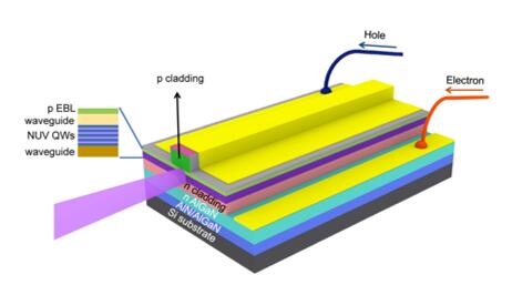
Figure 1. Schematic architecture of AlGaN-based NUV LD grown on Si. (Image by FENG Meixin)
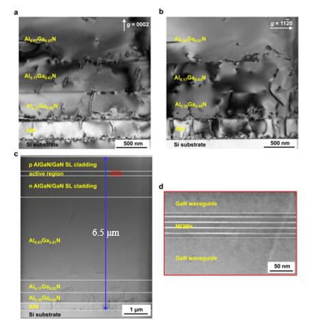
Figure 2. Cross-sectional TEM images of an AlGaN-based NUV laser grown on Si. (a), (b), Cross-sectional weak-beam bright-field TEM images of the AlN/AlGaN multilayer buffer
grown on Si obtained with diffraction vectors g = 0002 (a) and g = 1120 (b) revealing TDs with screw and edge components, respectively. (c) Cross-sectional high-angle annular dark-field scanning TEM image of an AlGaN-based NUV laser structure grown on Si. The thickness of the whole epitaxial structure was 6.5 μm. (d) Enlarged image of the In0.05Ga0.95N/Al0.1Ga0.9N NUV QW active region marked with red rectangle in (c). (Image by FENG Meixin)
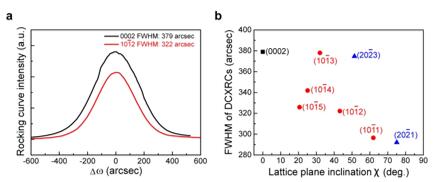
Figure 3. (a) DCXRCs around (0002) and (1012) planes of the Al0.03Ga0.97N template in the AlGaN-based NUV laser structure grown on Si, and (b) FWHMs of DCXRCs as a function of the lattice plane inclination angle of the Al0.03Ga0.97N template in the NUV laser structure grown on Si. (Image by FENG Meixin)
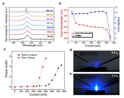
Figure 4. Electroluminescence (EL) characteristics of an as-fabricated AlGaN-based NUV LD grown on Si at room temperature. (a) EL spectra of an as-fabricated AlGaN-based NUV LD grown on Si before the cavity facet coating measured under various pulsed currents. (b) Peak wavelength and FWHM of the EL spectra of the LD before coating as a function of the pulsed injection current. (c) EL light output powers of the LD before and after the cavity facet coating as a function of the pulsed injection current. (d), (e), Far-field patterns observed below (0.9 Ith) (d) and above the threshold current (1.1 Ith) (e) by setting a sheet of white copying paper in front of the front facet of the NUV LD under pulsed currents (The pulse width was 400 ns, and the repetition rate 10 kHz) at room temperature, and a blue fluorescence formed when the NUV light illuminated the white copying paper. (Image by FENG Meixin)
Contact information:
Prof.SUN Qian,Suzhou institute of Nano-Tech and Nano-Bionics, Chinese Academy of Sciences.
Email: qsun2011@sinano.ac.cn
Reference: https://pubs.acs.org/doi/abs/10.1021/acsphotonics.7b01215
https://www.nature.com/articles/nphoton.2016.158
downloadFile