1.3 μm InAs/GaAs quantum dots (QD) lasers have exhibited a number of advantages over the commercial laser diodes of InP-based III-V QW structures, such as low threshold current, high quantum efficiency and high temperature stability, and hence have attracted great interests for the application of high speed fiber-optic communication systems.
For high-speed laser applications, a very short cavity length is crucial due to the significantly reduced lifetime of photons. However, it is very challenge to obtain a 1.3μm ground state (GS) lasing from a QD laser diode with a short cavity length owing to the low GS gain of QDs, which severely impede the high speed response characteristics of the device.
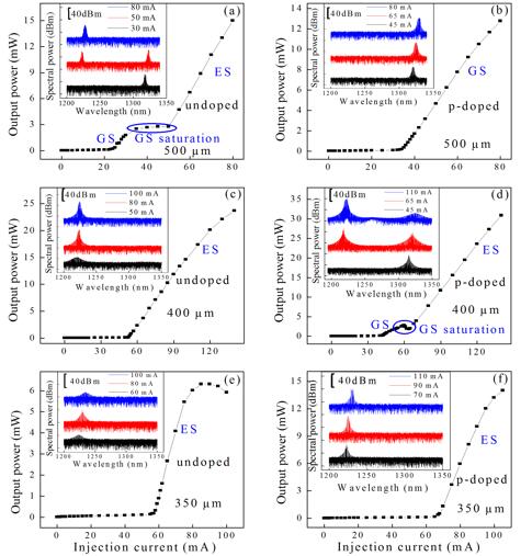
Recently, a research team led by Prof. ZHANG Ziyang from Key Laboratory of Nano-devices and Applications, Suzhou Institute of Nano-Tech and Nano-Bionics (SINANO), Chinese Academy of Sciences collaborated with Prof. NING Jiqiang from Nano-X, SINANO have successfully realized the 1.3μm GS lasing from a Fabry-Perot (F-P) QD laser with a 400 μm ultra-short cavity length without facet coating as shown in Figure.1.
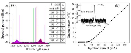
Additionally, as seen in Figure. 2, the single longitudinal mode lasing with a very large tunable range of 140 nm and side mode suppression ratio as large as 51 dB is achieved in a 500 μm long laterally coupled distributed feedback (DFB) QD laser diode.
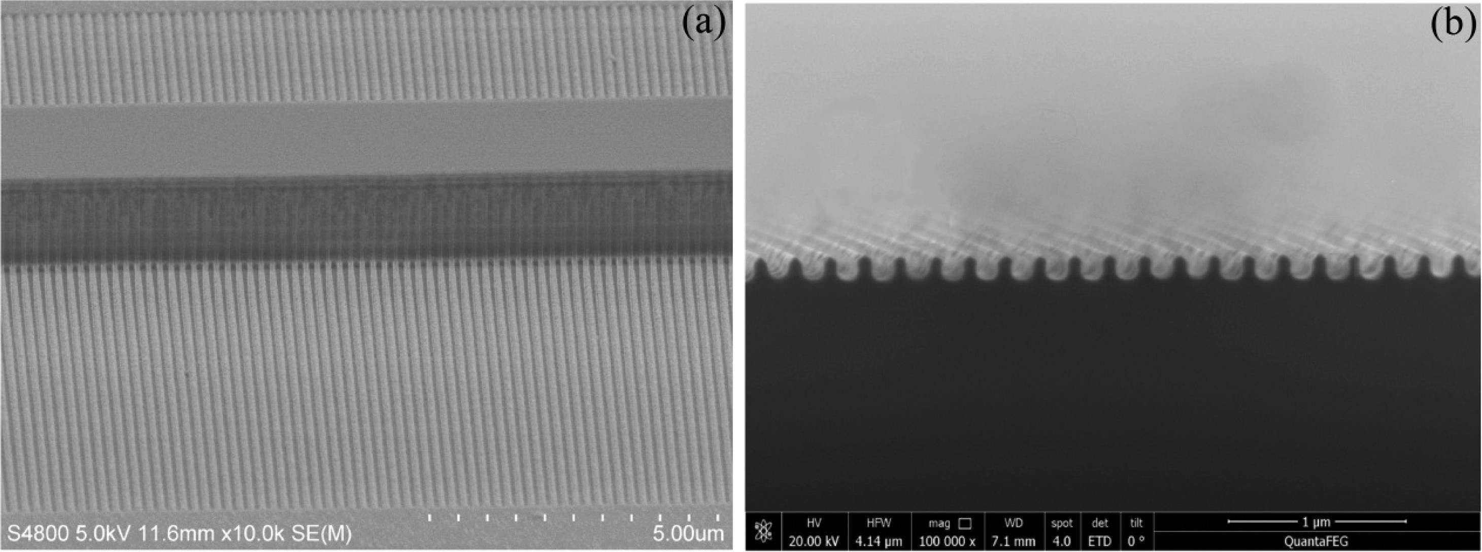
The high gain by modulation p-doping in the multiple InAs/GaAs QD structures and by a post-growth annealing process, as well as the optimized shallow etched laterally coupled DFB laser waveguide structure (as shown in Figure. 3) are believed to be the main reasons lead to the high performance of QD laser diodes.
This work demonstrates great potential of InAs/GaAs QD lasers for applications in high-speed fibre-optics communications.

Figure 1. P-I characteristics of the QD lasers with different L, measured under CW operation at RT; (a), (c), (e) are for un-doped QD lasers with 500, 400 and 350 μm; (b), (d), (f) are for p-doped QD lasers with 500, 400 and 350 μm respectively. Inset: The corresponding lasing spectra of the device under various injection currents.(Image by SINANO)

Figure 2. (a) Lasing spectra of modulation p-doped QDs DFB lasers with different grating periods. Inset:The detailed information of the LC-DFB lasers, including the lasing wavelengths, SMSR and Bragg periods. (b) P-I characteristic of p-doped QDs DFB laser under CW operation at RT. Inset: Lasing spectrum of p-doped QDs DFB laser measured at 1.8Ith.(Image by SINANO)

Figure 3. Top view of the SEM image of the LC-DFB laser structure with first-order grating. (b) Cross-sectional SEM image of grating after dry etching .(Image by SINANO)
Contact information:
Prof. ZHANG Ziyang, Suzhou institute of Nano-Tech and Nano-Bionics, Chinese Academy of Sciences.
Email: zyzhang2014@sinano.ac.cn
Reference: https://pubs.acs.org/doi/10.1021/acsphotonics.7b01355
downloadFile
