Recently Prof. YANG Hui and Prof. SUN Qian’s research group at Suzhou Institute of Nano-Tech and Nano-Bionics (SINANO), Chinese Academy of Sciences has published a paper in Nature Photonics, entitled "Room-temperature continuous-wave electrically injected InGaN-based laser directly grown on Si". In this paper, SINANO scientists reported the first demonstration of InGaN-based blue–violet laser directly grown on Si, operating under a continuous-wave current injection at room temperature.
Si is the most commonly-used material in the semiconductor industry. Si-based electronics and integrated circuits have been widely applied in various aspects in our daily living and work, from smart phones, computers to automobiles, airplanes and satellites. Given the exponential growth of the information industry, a global Internet traffic is set to increase dramatically and surpass the zettabyte (270 bytes) threshold soon. Hence broadband, high-density, high-speed data transmission at a low-cost is strongly desired for signal processing and high-performance computing. Optical interconnections via Si photonic technology have been widely recognized as a potential solution to overcome this bottleneck. Higher data rates and higher interconnection densities with lower system-level power dissipations could be obtained when using photons as the medium to detect, process, and transmit information. However, Si as an indirect band-gap material is hardly considered as an efficient light-emitting material. This remains as the key roadblock of Si photonics and its low-cost large-scale integration with Si electronics for decades, which recently has drawn renewed intense research interest. It’s highly desirable to grow III-V semiconductor laser directly on Si for a monolithic integration with Si photonics to take a full advantage of the low-cost high-yield fabrication foundries.
Besides the conventional III-V semiconductors, (Al, Ga, In)N light-emitting materials with a direct-band emission wavelength ranging from deep ultraviolet to near, infrared offer a new technical approach towards on-chip light source. Since the invention of the 1st InGaN-based laser diode in 1996, the past 20 years have witnessed its rapid development and application in information storage, laser lighting, laser display, visible light communication and biomedical diagnostics. Commercial GaN-based laser diodes are unambiguously grown on small-size, costly free-standing GaN substrates, which hinders their further commercialization. By utilizing large-diameter cost-effective Si substrates, the cost of GaN-based laser diodes can be slashed down dramatically, which will further expand its applications.
The hetero-epitaxial growth of GaN on Si encounters a large mismatch in both lattice constant and coefficient of thermal expansion, often resulting in a high density of defects and even micro-crack networks. By inserting a ‘hand-shaking’ buffer layer between Si and GaN, SINANO scientists have successfully tackled the problem and achieved crack-free high-quality GaN film on Si with a dislocation density less than 6 x 108 cm-2. Thanks to the excellent stress engineering and defect control, they have demonstrated the first operation of InGaN-based blue-violet (413 nm) laser directly grown on Si under a continuous-wave current injection at room temperature, with a threshold current density of 4.7 kA/cm2. A quick statistical analysis on the threshold current of the as-fabricated devices indicated a reasonable uniformity and reproducibility as the first demonstration. With a further improvement in material quality, device performance and lifetime, GaN-on-Si technology holds a strong hope in commercializing III-nitride LDs on large diameter Si with a cost down by orders of magnitude. Moreover, by growing GaN upon Si(111)-on-Insulator-Si(100), InGaN-based LDs as a new promising candidate for on-chip light source of Si photonics may pave the way for optoelectronic integration.
This project is supported by the Bureau of Frontier Sciences and Education, Chinese Academy of Sciences (CAS), the Strategic Priority Research Program of CAS, the National Natural Science Foundation of China, the National Key Research and Development Program of China, and the seed fund from SINANO, CAS.
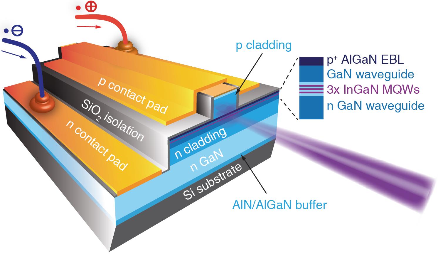
Figure 1.Schematic architecture of InGaN-based LD directly grown on Si.(Image by SINANO)
Contact information: Prof. SUN Qian
Suzhou Institute of Nano Tech and Nano Bionics, Chinese Academy of Science
Suzhou, Jiangsu 215125,China.
E-mail: qsun2011@sinano.ac.cn
downloadFile