Key Laboratory of Nanodevices and Applications, CAS
Key Laboratory of Nanodevices, Jiangsu Province
Profile
Driven by the national major strategic needs as well as technological innovation requirements of the rapid economic development, we are aiming to discover new device physical mechanisms and develop novel nanostructures. The current research interests focus on nano optoelectronic devices, nano electronic devices, nano electromechanical devices for the applications of energy and informations. Division of Nanodevices and Related Nanomaterials consists of 16 research groups, with over 150 staffs and graduate students.
Mission
Key Laboratory of Nanodevices and Applications takes advanced device technologies in "post Moore era" as the long-term goal. We focus on the development and application of III-N, III-V, and carbon based-IV semiconductors based nanodevices, including the frontier research of nanostructures and nanodevice physics, technological research and development of key material growth and device processing, as well as heterostructure integration research and system applications. Meanwhile, we strive to form a certain international influence in the talent team construction, independent design and implementing equipment of nano-testing and characterization, the core technology research and development and transformation of nano-devices.
Research Areas
1. Low dimensional heterostructures and devices based on III-N compound semiconductor
GaN based materials, as the third generation semiconductor materials, including GaN, AlN and InN and their alloys, are direct band gap semiconductors, which are ideal materials for the fabrication of semiconductor lasers from UV to visible light. GaN based laser has been widely used in the fields of laser display, laser illumination, communication and so on. This direction includes (1) high quality GaN self-supporting substrate, (2) GaN based blue/green laser and LED, (3) GaN based Terahertz devices and power electronic devices based on the two-dimensional electron gas.
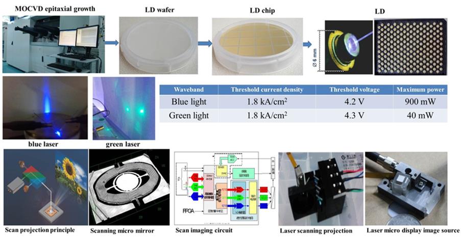
Fig.1 GaN based blue/green laser and laser display.(Image by SINANO)
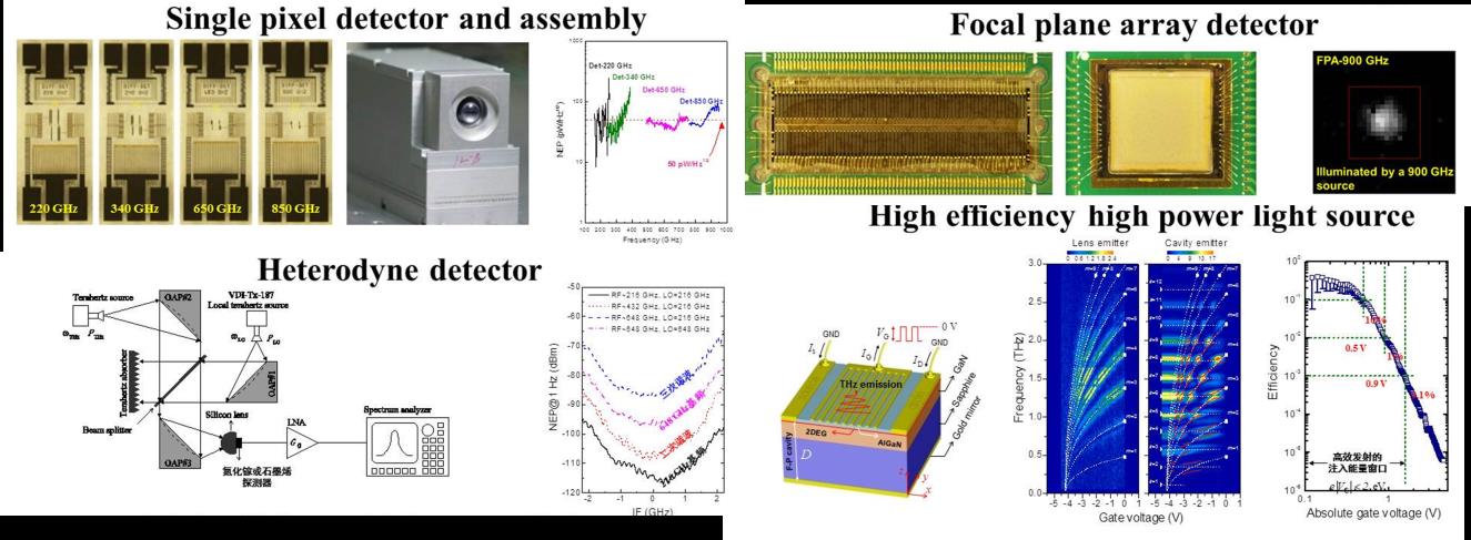
Fig.2 GaN based Terahertz devices.(Image by SINANO)
Fig.3 GaN based HEMT power electronic devices.(Image by SINANO)
2. Quantum structure growth and device based on III-V compound semiconductor
III-V compound semiconductors with high saturation velocity, wide band gap and adjustable energy band have played a key role in the development of large-capacity information transmission and high-speed signal processing system. This direction includes (1) high-speed real random number generator based on semiconductor superlattice, (2) high-efficiency multi-junction solar cell based on III-V compound semiconductor, (3) infrared materials and detectors.
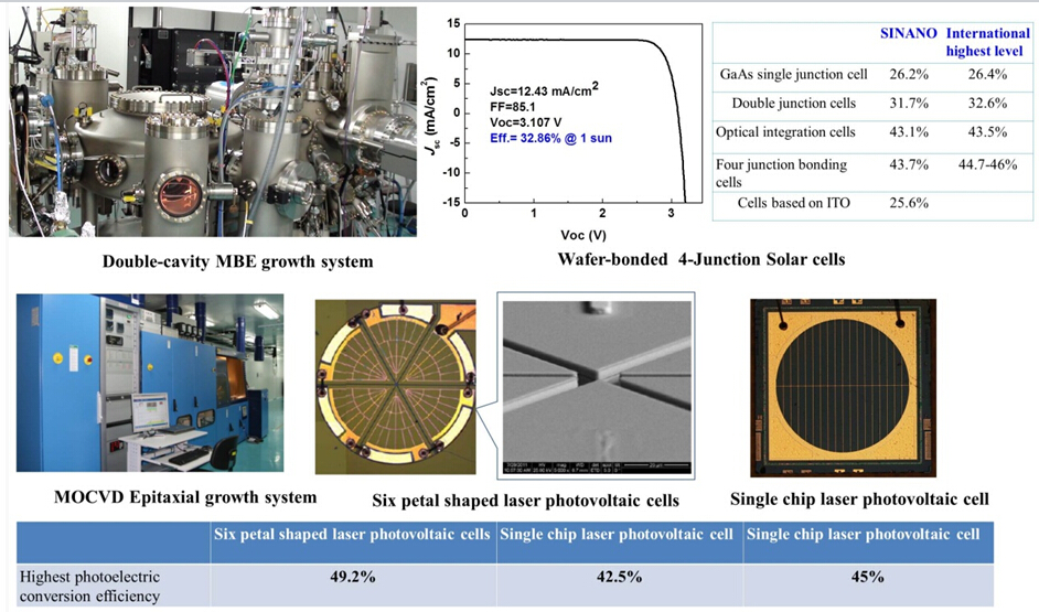
Fig.4 High-efficiency multi-junction solar cell.(Image by SINANO)
3. Nano materials and device applications based on carbon
This direction includes research on (1) well-controlled scalable growth techniques for carbon nanomaterials, (2) carbon nanocomposite, (3) functional carbon nanomaterial and devices. Especially for carbon nanotube electronic devices, the emphasis is on the development of the related macro separation technology and the applications of the devices.
Carbon nanotube thin film transistor devices need to meet high mobility, high switching ratio, high current density and high uniformity, in order to promote their applications in electronic and optoelectronic devices. The key technology is to achieve high purity and high quality semiconductor single wall carbon nanotubes.
4. Measurement and analysis method of nanoscale multi physical quantity
This direction includes (1) measurement of the local optical properties at nano scale, (2) near field optical detection of single molecules and nanostructures, (3) test and characterization methods for far infrared / terahertz / sub millimeter wave high frequency optoelectronic devices.
Developed scanning near-field optical probe system by using scanning probe microscope as the core, optical excitation and detection system is coupled to the vicinity of the tip. A photoelectric chemical electrolytic tank is developed, which is specially used in the scanning head part. It is used to realize the measurement of near field optics, surface photo voltage / current and solid-liquid interface by nano scale spatial resolution.
Core Facilities
The lab space is more than 3500 square meters, including 16 professional physics labs, 3 professional chemical labs, and one super-clean lab. Six MOCVDs and one dual-chamber MBE for material growth are installed in the super-clean lab.
Contact Information
Prof. QIN Hua
Tel: +86-(0)512-62872567
E-mail: hqin2007@sinano.ac.cn
Ms. REN Xin
Division secretary
Tel/Fax: (+86) 512-62872640
Email: xren2011@sinano.ac.cn
Address: Division of Nanodevices and Related Nanomaterials
Suzhou Institute of Nano-Tech and Nano-Bionics (SINANO), CAS
398 Ruoshui Road, Suzhou, 215123


