As a third-generation semiconductor material, GaN is now widely applied in optoelectronic fields, such as light emission diodes (LEDs), ultraviolet detectors, laser diodes (LDs) and high electron mobility transistors (HEMT). Besides, due to its advantages of high radiation resistance and good chemical stability, GaN also has excellent potentials in nuclear radiation detection. There was few investigation of GaN for X-ray detection until recently, which will bring a great prospect of Fe-doped GaN based X-ray detectors due to its very low leakage current.
Dr. LU Min's team applied the Fe-doped GaN wafer supplied by Suzhou Nanowin Science & Technology Co.,Ltd and succeeded in fabricating the prototype device of X-ray photoconductive detectors. The detectors have vertical structure with upper and lower electrodes. With the applied bias as high as 200V, the ratio of X-ray photo current to dark current is up to 180 without shading environment. And clear X-ray scanning imaging of hexagonal steel nuts can be realized applying our detecors. Besides, the research paper about the detector has been published in the magazine “Physica Status Solidi: Rapid Research Letters" (No. 5–6, 187–189 (2011) / DOI 10.1002/pssr.201105163). One reviewer considered that this study is interesting and does highlight the potential of Fe doped GaN for radiation detection. It is known that, it is the first-time that X-ray detectors based on Fe-doped GaN photoconductors was internationally reported.
This study is supported by the National Natural Science Foundation of China (Grant No. 10875084), the Natural Science Foundation of Jiangsu Province (Grant No. BK2008174) and the Applied Science Foundation of Suzhou (Grant No. SYJG0915).
 |
|
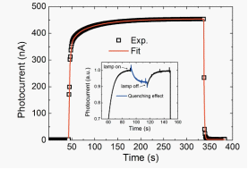
Figure 1: Typical photo-current transient of the GaN photoconductor (black open squares);
Its fitting result (red line) when the X-ray source is turned on and off at 200V.
The inset shows the optical quenching effect (blue section) on the Fe doped GaN photoconductor.
Figure by SINANO |
 |
|
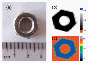
Figure 2 (online color at: www.pss-rapid.com)
(a) Optical photograph of a steel hex nut;
(b) X-ray scanning gray scale image;
(c) X-ray scanning color fill map of this steel hex nut.
Figure by SINANO |


