Recently, Suzhou Institute of Nano-Tech and Nano-Bionics (SINANO), CAS successfully developed a normally off AlGaN/GaN/Si HEMT power switching device. The device shows good gate input swing of 15 Volt and high threshold voltage of 3.5 Volt, which has reached the international advance level. It is also the first time in China that the GaN/Si power switching device is reported.
Owing to the excellent material properties such as high electron mobility and high breakdown field, GaN-based semiconductors are well suited for next-generation power switching devices. It is expected that the power conversion systems using GaN power switches can achieve 3.5% to 7% efficiency improvement with volume shrinkage of about 35%. Recent progress in GaN epitaxial growth technology allowed the fabrication of GaN-on-Si wafers with high quality, low cost, and large wafer size of up to 6 inch. Based on the GaN-on-Si technology platform, field-effect transistors (FETs) can be produced in large volume. Many world famous power devices manufacturers such as, IR, Infineon, Fairchild, Samsung are focusing on development of GaN/Si power switches. According to Yolo’s analysis, the market of GaN power devices will reaches 0.35 billion USD in 2015, then increase sharply in the following several years. In next decade, GaN power device will become a strong competitor to traditional Si power device, and share discrete power devices market of ten billion USD per year currently.
Fabrication of GaN/Si power switching device is really a tough work, including material epi-growth, chip process and package. There are so many technical barriers need to overcome, for instance, high quality GaN epi-growth on large Si substrate, normally off operation with higher threshold voltage more than 3V and large gate input swing. Though small devices have already been demonstrated by many research teams all around world, however, a few companies could show large devices with high current more than 5 ampere owing to the sophisticated process controlling.
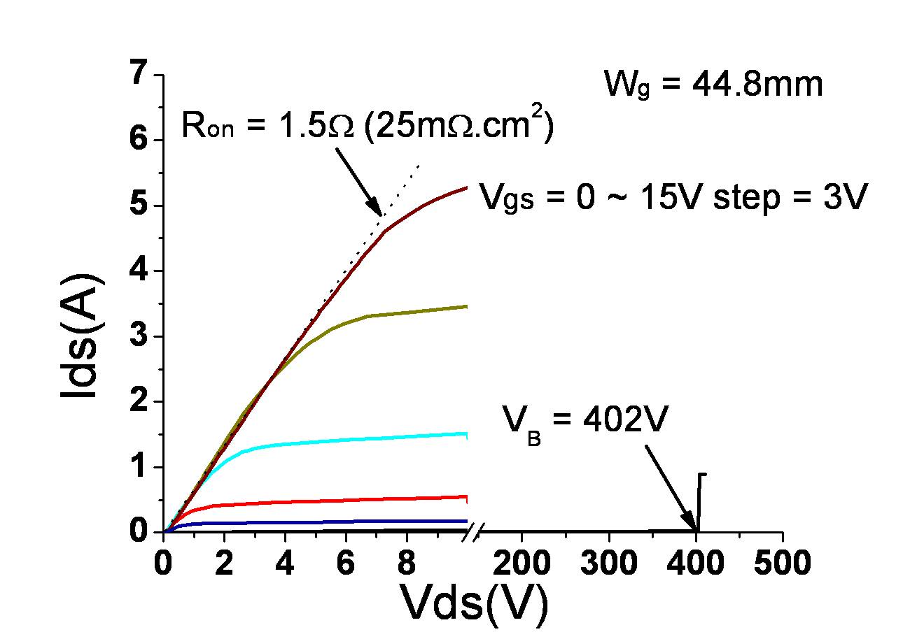
SINANO started the GaN/Si high power switching devices from 2010. The team invited Professor Kevin J. Chen of HKUST as technical consultant, who is a famous scientist in compound semiconductor devices. They also had cooperation with Suzhou Silikron Semiconductor Company. By overcoming the key technical problems and developing some unique technologies, the threshold voltage of the power switching devices reaches 3.5 Volt, maximum output current reaches 5.3 Amp, and pinch-off breakdown voltage reaches 402 Volt. It should be noted that this device shows good gate input swing (15 Volt). The high threshold voltage of 3.5 Volt and large gate input swing of 15 Volt enable the direct replacement of traditional Si power devices by this device in power conversion systems.
 |
|
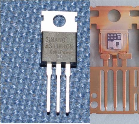
Figure 1: AlGaN/GaN/Si power switching device
Image provided by SINANO |
 |
|
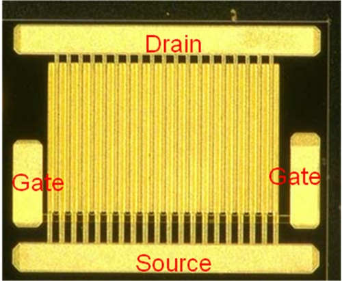
Figure 2: Optical photo of device chip
Image provided by SINANO |
 |
|
Output characteristics of AlGaN/GaN/Si HEMT power switches
Image provided by SINANO |


