Chemical vapor deposition (CVD) provides a synthesis route for large-area and high-quality graphene films. However, layer-controlled synthesis remains a great challenge on polycrystalline metallic catalysts due to the self-limited nature of carbon on Cu surface and the larger carbon solubility in Ni.
Recently, Prof. LIU Liwei's group from Key Laboratory of Nano-devices and Applications, CAS, in collaboration with the Institute of Physics, CAS, has successfully developed a novel synthesis technique to achieve layer-controlled growth of graphene. For conventional CVD graphene films (CVDG) on Ni surface, the process generally involves the dissociation of the hydrocarbon, the dissolution and diffusion of carbon in Ni and the formation of graphene. The formation of graphene films probably contains the several dynamic processes: metal-induced crystallization at high temperature, segregation at the interface and precipitation at grain boundaries during cooling. Intertwinement of these complicated processes, especially the precipitation at grain boundaries, will result in the non-uniformity and the uncontrollable layers of graphene films. Prof. LIUand co-workers have achieved a facile and viable synthesis of layer-controlled and high-quality graphene films on wafer-scale Ni surface by the sequentially separated steps of gas carburization, hydrogen exposure, and segregation (Figure 1). H2 exposure assisted by Ni film at high temperature plays critical roles not only in the removal of the carbon layers formed in the initial CVD carburization process but also in the effective reduction of the carbon mount in Ni for promoting the sequential segregation process. The number of layers is precisely controlled by changing Ni film thickness, gas carburization amount and H2 exposure dose (Figure 2). Excellent electrical and transparent conductive performance, with a room-temperature mobility of ~3000 cm2V−1s−1 and a sheet resistance as low as ~100 Ω per square at ~ 90% transmittance, of the twisted few-layer grapheme films grown on the Ni catalyst is demonstrated. The findings open a feasible route towards control over the layer number of wafer-scale graphene, new understanding of the graphene formation on Ni catalyst, and eventual diverse applications of graphene-based devices. This work has been published on Adv. Funct. Mater. 2012, 22, 3153–3159.
The work was supported by NSFC and MOST projects. The project also got assistance from the Nanofabrication Facility and Platform of Characterization & Test of SINANO.
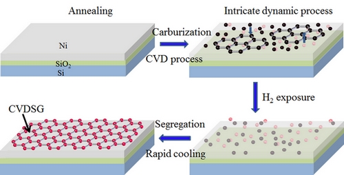 |
| Figure 1. Schematic diagrams of synthesis processes of CVDSG films. |
 |
|
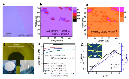
Figure 2.Uniformity and layer-controlled of wafer-scale CVDSG
a) Optical image of the CVDSG film.
b,c) I2D/IG (b) and W 2D (c) Raman mapping of CVDSG films (1–2 layers).
d) 2-inch graphene film (left inset) is released in a mild FeCl3 aqueous solution and is transferred onto the PET flexible substrates (right inset).
e) Optical transmittance of CVDSG films. f) Electron transport of a graphene Hall bar device (inset). |


