Single-walled carbon nanotubes (SWCNTs) have been widely regarded as one of the ideal materials for energy devices, sensors, transparent electrodes, and electronics due to its extraordinary physical, chemical and mechanical properties. For making field effect thin-film transistors (TFT), semiconducting SWCNTs (sc-SWCNTs) are the primary materials which are of high carrier mobility (mobility of individual sc-SWCNT is of ~10
4 cm
2 V
-1s
-1) and can be dispersed well in some organic solvents and aqueous solutions with the aid of sonication, therefore, are one of the most promising semiconducting materials for preparing high-performance printed TFTs and circuits.
In the last few years, Printable Electronics Research Center (PERC) at Suzhou Institute of Nano-tech and Nano-bionics has been focusing on developing high-quality printable sc-SWCNT inks and fabricating high-performance flexible printed TFTs and circuits, such as OLED driving circuits, logic gates and circuits. Up to now, we have developed more than 10 types of high-quality printable sc-SWCNT inks, and successfully fabricated high-performance printed TFTs and circuit arrays on the flexible substrates using the developed inks. As shown in Figure 1, printed SWCNT TFTs show excellent properties with on/off ratio up to 107 and mobility more than 30 cm2V-1s-1; at the same time, the uniformity of printed TFTs has also been greatly improved by optimizing the printing technologies. (ACS Appl. Mater. Interfaces, 2014, 6(13), 9997-10004, http://pubs.acs.org/doi/abs/10.1021/am502168x).
Printed OLED driving circuit arrays are successfully fabricated on the PET substrate (Figure 2), and all of them can control the light output of OLED due to their high output currents and good on/off ratios at low voltage. (Figure 3) (Nanoscale, 2014, 6(3): 1589-1595; http://pubs.rsc.org/en/Content/ArticleLanding/2014/NR/c3nr04870e#!divAbstract)
Printed flexible inverters show good performance with voltage gain up to 33 with 1.25 V voltage, and can work at 10 kHz. The frequency of printed flexible five-stage ring oscillators can reach 1.7 kHz at voltages of 2 V with per stage delay times of 58.8 μs. (Figure 4) (Nanoscale, 2014, DOI: 10.1039/C4NR05471G http://pubs.rsc.org/en/content/articlelanding/2014/nr/c4nr05471g#!divAbstract). Work is underway at PERC to construct backplane driving electronics for flat panel displays and high-performance logic gates and circuits based on printed SWCNT TFTs.
This work was supported by Natural Science Foundation of China (91123034, 61102046), Strategic Priority Research Program of the Chinese Academy of Science (XDA09020201), the Knowledge Innovation Programme of the Chinese Academy of Sciences (KJCX2-EW-M02) and Basic Research Programme of Jiangsu Province (BK2011364 ).
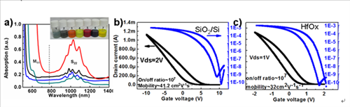
Figure 1. Absorption spectra of printable sc-SWCNT inks (a) and electrical properties of printed TFTs on different substrates using as-prepared sc-SWCNT inks (b,c). (ACS Appl. Mater. Interfaces, 2014, 6(13), 9997-10004)
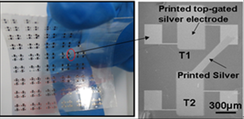
Figure 2. Optical image of Printed OLED driving circuit arrays based on printed top-gate TFTs on the PET substrate. (Nanoscale, 2014, 6(3): 1589-1595)
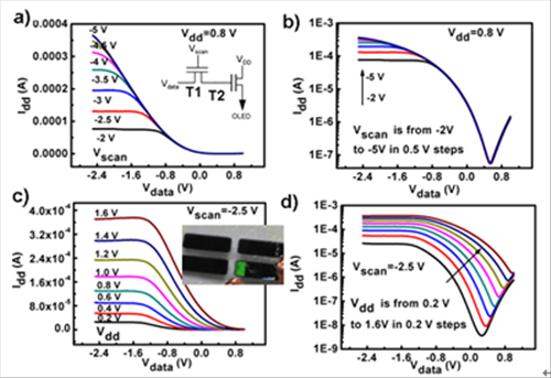
Figure 3. The relationships of output currents and voltages of printed driving circuits on the flexible substrates. (Nanoscale, 2014, 6(3): 1589-1595)
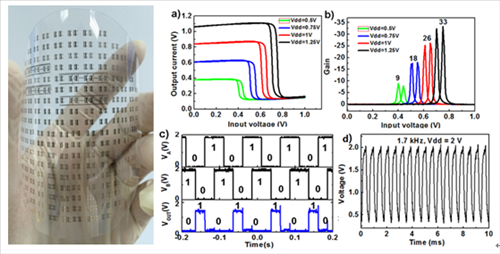
Figure 4. Optical image of printed inverter, NOR and ring oscillator arrays on the flexible substrate, and electrical properties of a printed inverter (a, b), NOR (c) and 5-stage ring oscillator (d). (Nanoscale, 2014, DOI: 10.1039/C4NR05471G)


