Solution-processed silver nanowire (Ag NW) networks have been widely used as transparent or stretchable conductor in touch panels, solar cells, displays, heaters, sensors, and other electronics. However, most of reported conductive Ag NW networks were deposited without pattern, which need additional patterning procedures such as etching for practical applications. Printing Ag NW directly to form conductive pattern, which is simplified and low-cost compared with depositing-etching methods, is difficult due to the unique dispersion properties of the metal nanowires. With respect to Ag NW electrode for organic photovoltaic (OPV), most of Ag NW networks were used as bottom electrode and organic layers were deposited on top of it. Only a few papers reported Ag NW as top electrode in OPV through lamination, spray, or drop-casting approaches, none of which researched the solvent effect to the underlying layers.
A team led by Prof. CUI Zheng from Printable Electronics Research Centre, Suzhou Institute of Nano-Tech and Nano-Bionics, developed conductive Ag NW networks pattern by inkjet printing. Then they inkjet printed Ag NW directly as top electrode for semi-transparent OPV devices by co-working with group of Prof. MA Changqi. The work was recently released in Appl. Phys. Lett. (doi: 10.1063/1.4913697).
The researchers obtained Ag NW patterns with different sheet resistance and transparency by adjusting inkjet printing parameters. The highest power conversion efficiency (PCE) of OPV device using transparent printed Ag NW as top electrode was achieved to be about 90% of the reference device’s PCE , which was fabricated using thermal deposited Ag opaque electrode.
On the other hand, a series of different OPV device were designed, and their current density-voltage (J-V) curves were studied carefully by comparing fabricating process. The results revealed that solvent treatment on the underlying layer during printing led to a decrease of charge injection selectivity and an increase of charge recombination at the anode interface, which was considered to be the reason for the degrading of device performance.
This work was supported by the projects from the National Natural Science Foundation of China, Chinese Academy of Sciences, and the National Science and Technology Ministry.
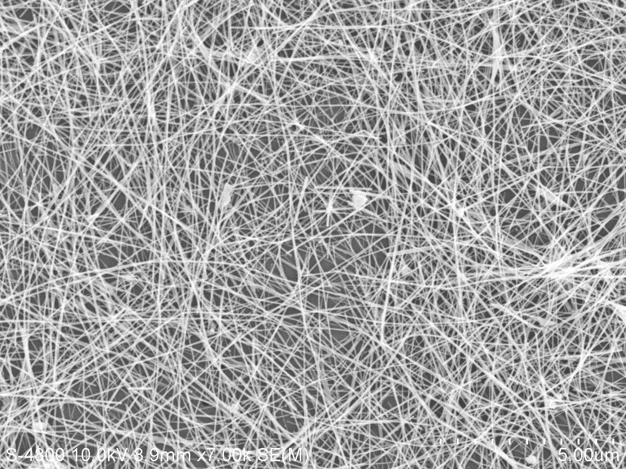
Figure1. A typical SEM image of the inkjet printed Ag NW.(Image by Prof. CUI Zheng's group)
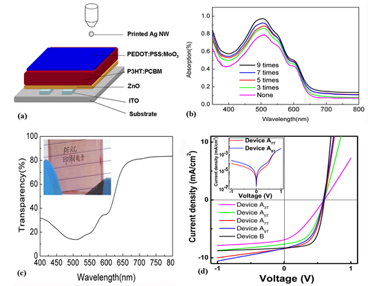
Figure 2. (a) The schematic structure of the inverted device with printed Ag NW electrodes, (b) the absorption of device before and after printing Ag NW, (c) the transparency of an OPV device with the picture in the inset, and (d) typical J-V characteristics of the OPV devices with inkjet printed Ag NW top electrode and thermal deposited Ag top electrode. The inset in figure (d) shows the comparison of dark J-V curves.(Image by Prof. CUI Zheng's group)


