Nanomaterials are increasingly used in wide areas of applications ranging from electronic, optoelectronic, bioelectronic, to sensing and energy nanodevices. Understanding the electrical properties of nanomaterials thus becomes not only a pursuit in basic science but also of widespread practical needs. The conventional field-effect transistor (FET) approach suffers from the complicated device fabrication process, non-Ohmic contact in many cases, and the low throughput.
Prof. CHEN Liwei's group in the Suzhou Institute of Nano-Tech and Nano-Bionics (SINANO), Chinese Academy of Sciences (CAS) and collaborators have developed a new functional scanning probe imaging mode, Dielectric Force Microscopy (DFM), to address these challenges. A recent review was published on Accounts of Chemical Research 48:1788 (2015)
Since mobile charge carrier polarization dominates the dielectric response to external electric fields in semiconducting and metallic materials, carrier concentration and mobility determines both the dielectric response and the electrical conductivity. The DFM functional imaging mode measures the dielectric polarization with high sensitivity force detection (~pN). Effectively, this imaging mode can “see” mobile charge carriers in nanomaterials without the need for direct electrical contact (Figure 1a). Using single-walled carbon nanotube (SWNT, diameter ~ 1 nm) and ZnO nanowire (diameter 30-50 nm) as model systems, the DFM technique is exploited to determine the dielectric constant [Nano Letters 7:2729 (2007)], semiconducting or metallic nature [Nano Letters 9:1668 (2009)], and in the semiconducting case, the carrier type [Journal of Physical Chemistry C 116:7158 (2012)] (Figure 1e-g). Interestingly, DFM technique show a spatial resolution of ~ 20 nm, which is previously not achievable with FET transport measurements.
Furthermore, Prof. Liwei Chen and collaborators demonstrate the parallel between DFM and FET characterization methods by direct comparison between DFM and FET measurements on the exact same SWNTs [Nano Research 7:1623 (2014)]. The results reveal that the DFM gate modulation, which is the ratio of DFM signal strengths at different gate voltage, is linearly proportional to the logarithm of FET device on/off ratio (Figure 1b). A microscopic Drude-level model is established to interpret this semi-logarithm correlation (Figure 1c). This model will be highly helpful in designing future measurements and applications using DFM.
In the broad context of electrical property measurements, the DFM technique is a “sister technique” to another scanning probe technique developed by Prof. Zhi-Xun Shen at Stanford University, scanning near-field microwave microscopy [Review of Scientific Instruments 79:063703 (2008)]. The two techniques share common features such as contact-less measurements, and with nanometer scaled spatial resolution, and they are complementary in the sense that the near-field microwave technique measures high-frequency dielectrics but the DFM technique measures low frequency to near-dc dielectrics. The DFM technique does not require costly high-frequency network analyzer or special probe tip, and is easily adaptable to various imaging environments. Future applications in both fundamental research and industrial on-line monitoring are expected to flourish.
This series of research are funded by the National Natural Science Foundation of China, Strategic Priority Research Program of the Chinese Academy of Sciences, Natural Science Foundation of Jiangsu Province, American Chemical Society Petroleum Research Fund, and Collaborative Innovation Center of Suzhou Nano Science and Technology.
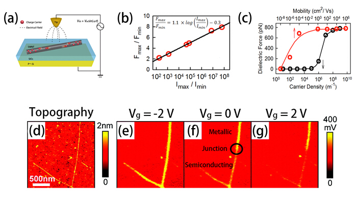
Figure 1. (a) Schematic illustration of the double-passed scan operation of DFM. (b) The semi-logarithm correlation between the gate modulation ratio in DFM and the on/off ratio in FET. (c) Numerical simulation showing the dependence of DFM signal on carrier density and mobility. The topographical (d) and dielectric response (e−g) images of a SWNT with an M−S intratube junction showcasing the spatial resolution of the DFM technique.(Image by CHEN Liwei's group)
Contact information:Prof.CHEN Liwei
Suzhou Institute of Nano Tech and Nano Bionics ,Chinese Academy of Science
Suzhou,Jiangsu 215125,China.
E-mail:lwchen2008@sinano.ac.cn


