High-efficiency solar cells used in concentrated photovoltaics (CPV) are usually based on GaAs material system such as InGaP/GaAs/Ge triple-junction solar cells or based on wafer bonding technology combining both GaAs- and InP-based subcells such as InGaP/GaAs//InGaAsP/InGaAs four-junction solar cells. Recently Dr. HUANG Yong's group at Suzhou Institute of Nano-tech and Nano-bionics, Chinese Academy of Sciences has proposed a novel InP-based monolithic metamorphic five-junction solar cells that could achieve high efficiency under solar concentration while still compatible with current growth technology. (Semicond. Sci. Technol. vol30, 105031, 2015)
In the proposed InP-based structure, three bottom subcells are composed of lattice-matched InGaAsP materials, while two top subcells employ metamorphic InGaP materials. The two InGaP subcells are designed to have a same Ga composition of 30%. The first InGaP subcell is thinned so as to transmit half of the photon flux to the second InGaP subcell, thus to form an upright five-junction InGaP(1.64eV)/InGaP(1.64eV)/InGaAsP(1.3eV)/InGaAsP(1.02eV)/InGaAs(0.74eV) solar cell structure on InP substrate. Assuming a unit conversion efficiency, each of the three bottom subcells generates a photocurrent of 10.65 mA/cm2 and the two top subcells share the remaining 21.3 mA/cm2, thus reaching a current match condition. Because no Al- or N-contained materials are used in the absorbers and only one metamorphic growth is required (with a lattice mismatch of 2.1%), the novel InP-based solar cell architecture is considered practically achievable with the current growth technology.
In addition, the upright structure of this design greatly simplifies the material growth and device processing and avoids any extra steps and costs associated with substrate removal and handle/wafer bonding in the wafer bonding architecture.
The maximum efficiency of this InP 5J cell that can be practically achieved is also estimated. By comparing relatively to the InGaP/GaAs/Ge reference cell and adding additional nonideal factors in the modeling, an efficiency as high as 46.2% is estimated under concentration at ~1500 suns. At this point, the InP 5J cell would produce a Jsc of 15.0 A/cm2 or 111.4 mA/W, a Voc of 4.94 V, and a FF of 0.84. The high efficiency, high concentration as well as the simplified processing are very promising for future CPV application. The calculated efficiencies for different solar cell architectures along with the highest reported/projected values are summarized in Table.1.
This work is supported by Hundred Talents Program from Chinese Academy of Sciences.
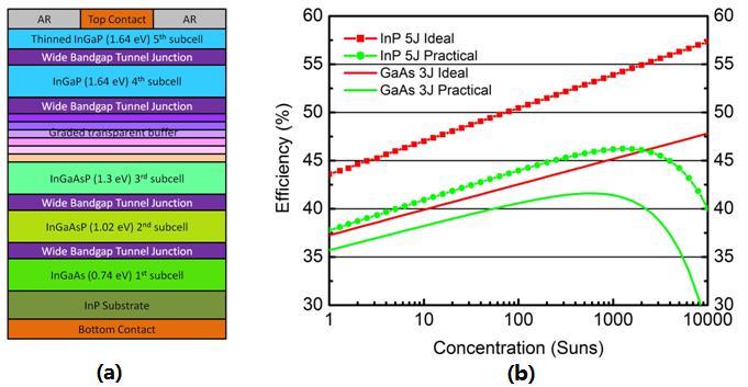
Figure1. (a) Schematic structure of the InP-based 5J solar cell; (b) The ideal (red) and practical (green) efficiency for InP 5J cell (square) and GaAs 3J reference cell (line) under concentration.(Image by HUANG Yong's Group)

Table 1 Summary of the calculated and highest reported/projected efficiencies for different multijunction solar cell architectures.(Image by HUANG Yong's Group)


