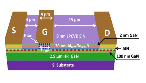
AlGaN/GaN HEMTs are promising candidates for high-frequency power amplifiers and power switching applications. Normally-off operation is highly desirable in high-voltage power switching applications because of the fail-safe requirement in a power conversion system, but it is difficult to achieve due to strong spontaneous and piezoelectric polarization in conventional AlGaN/GaN heterojunctions grown on Si substrate. Meanwhile, the HEMT has small threshold voltages and small gate swings that are limited by the Schottky-gate forward turn-on voltages. By inserting a gate dielectric such as SiNx, MIS-HEMTs can deliver suppressed gate leakage and enlarged gate swing, and are preferred over HEMTs for power switching applications.
Recently, Prof. ZHANG Baoshun’s group, at Suzhou Institute of Nano-tech and Nano-bionics, Chinese Academy of Sciences presents a fabrication technology of enhancement-mode (E-mode) AlGaN/GaN metal-insulator- semiconductor high electron-mobility transistors (MIS-HEMTs) using 10 keV fluorine ion implantation. An 8 nm low pressure chemical vapor deposition (LPCVD) silicon nitride layer was deposited on the AlGaN as gate dielectric and energy-absorbing layer that slows down the high energy (10 keV) fluorine ions to reduce the implantation damage. For SiNx thin film deposition, compared with some commonly used methods (e.g. plasma enhanced chemical vapor deposition (PECVD) and inductively coupled plasma chemical vapor deposition (ICP-CVD)), low temperature chemical vapor deposition (LPCVD) is free of plasma induced damage and yields Si3N4 film with higher quality and higher thermal stability owing to higher deposition temperature. The E-mode MIS-HEMTs exhibit a threshold voltage as high as + 3.3 V with a maximum drain current over 200 mA/mm (250 mA/mm for depletion-mode (D-mode) MIS-HEMTs) and a high on/off current ratio of 109. Meanwhile, the E-mode MIS-HEMT dynamic RON is only 1.53 times larger than the static RON after off-state VDS stress of 500 V. This work has been published in the journal Electron Device Letters, IEEE , 36(11): 1128 – 1131.
This work was partly supported by the Key Technologies Support Program of Jiangsu Province (grant No. BE2013002-2). And the authors are grateful for the technical support provided by Nanofabrication Facility and Platform for Characterization and Test of SINANO, Chinese Academy of Science.