To obtain higher efficiencies, both the lattice-matching conditions and the current matching conditions between the subcells that compose the multi-junction solar cell structure should preferably be satisfied. However, in the case of four or more junctions, dislocations resulting from metamorphic buffers in the upright lattice-mismatched growth would deteriorate the device performance. Direct wafer-bonding offers the possibility to integrate lattice-mismatched subcells from different substrates into a single device. Most of reported wafer-bonding techniques need high-temperature annealing, which could result in wafer bending and void formation at the bonding interface owing to the different thermal expansion coefficients of different materials. Room-temperature wafer-bonding technique can avoid these problems. With respect to material growth, MOCVD technique is conventionally used for the epitaxial growth for the solar cells. The research of solar cell by using MBE is scarce. Our previous work suggests that growth using solid-state molecular beam epitaxy (MBE) is possible to improve material quality and to control the high doping of tunnel junction structure. A team led by Prof. LU Shulong from Key Laboratory of Nanodevices and Applications, Suzhou Institute of Nano-Tech and Nano-Bionics, developed room-temperature wafer-bonded InGaP/GaAs//InGaAsP/InGaAs four-junction solar cell grown by all-solid state MBE. The room temperature wafer bonding technique for GaAs and InP was fabricated by co-working with group of Prof. Shiro Uchida from Chiba Institute of Technology. The work was recently published in Applied Physics Express 9, 016501 (2016). An InGaP/GaAs tandem cell on a GaAs substrate and an InGaAsP/InGaAs tandem cell on an InP substrate were grown separately by all-solid state MBE. The room-temperature direct wafer-bonding technique was used to integrate these subcells into an InGaP/GaAs//InGaAsP/InGaAs wafer-bonded solar cell, which resulted in an abrupt interface with low resistance and high optical transmission. The current matching design for the base layer thickness of each cell was investigated. Based on the current matching design, the resulting efficiency of the four-junction solar cell was 42.0% at 230 suns, which demonstrates the great potential of the room-temperature wafer-bonding technique to achieve high conversion efficiency for cells with four or more junctions. This work was financially supported by the National Natural Science Foundation of China and the knowledge Innovation Project of the Chinese Academy of Sciences. 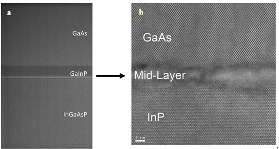
Figure 1, Cross-sectional transmission electron microscopic (TEM) image of the bonded interface (a) and the high resolution TEM image of the interface of GaAs and InP (b). (Image by Prof. LU Shulong's group) 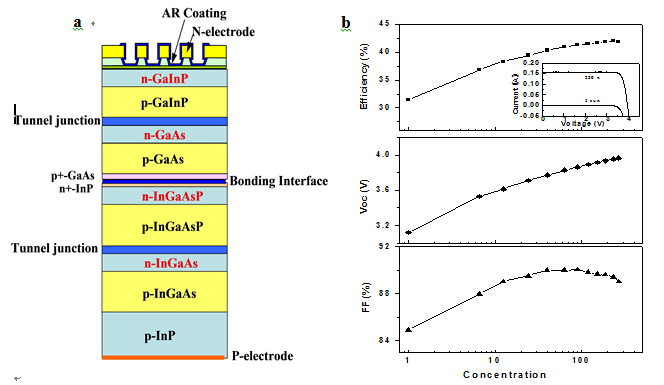
Figure 2 The schematic structure of the device structure (a); The efficiency, Voc and FF as a function of concentration. Inset shows I-V curves of the 4-junction solar cell at 1-sun and under concentration (b). (Image by Prof. LU Shulong's group) Contact information:Prof.LU Shulong Suzhou Institute of Nano Tech and Nano Bionics ,Chinese Academy of Science Suzhou,Jiangsu 215123,China. E-mail:sllu2008@sinano.ac.cn |


