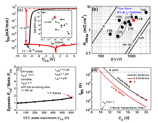
Gallium nitride (GaN)-based high electron mobility transistor (HEMT) power devices have demonstrated great application potential due to high current density, high switching speed, and low ON-resistance in comparison to the established silicon (Si)-based semiconductor devices. These superior characteristics make GaN HEMTs emerge as promising candidates for next-generation power converters. Recently, Prof. ZHANG Baoshun's group, at Suzhou Institute of Nano-tech and Nano-bionics, Chinese Academy of Sciences,reveals high performance AlGaN/GaN MIS-HEMTs. The gate dielectric layer and surface passivation layer are formed by the low pressure chemical vapor deposition (LPCVD) Si3N4. The LPCVD-Si3N4 MIS-HEMTs exhibit a high breakdown voltage 1162 V at IDS = 1 µA/mm, a low OFF-state leakage of 7.7 × 10⁻¹² A/mm and an excellent ON/OFF current ratio ~ 1011. Compared with the static ON-resistance of 2.88 mΩ·cm2, the dynamic ON-resistance after high OFF-state drain bias stress at 600 V only increases to 4.89 mΩ·cm2. The power device figure of merit (FOM = BV2/RON.sp) is calculated as 469 MW·cm-2. The LPCVD-Si3N4/GaN interface state density is in the range of (1.4-5.3) × 1013 eV-1 cm-2 extracted by conventional conductance method. Finally, the gate insulator degradation of GaN-based MIS-HEMTs is analyzed by time-dependent-dielectric breakdown (TDDB) test. The lifetime is extrapolated to 0.01% of failure after 10 years at 300 K by fitting the data with a power law to gate voltage of 10.1 V. These results prove a great potential of LPVCD-Si3N4/AlGaN/GaN/Si MIS-HEMTs for high power switching applications.This work has been published in the journal Electron Devices, IEEE Transactions on, 2015, 63(2): 731 - 738. This work was partly supported by the Key Technologies Support Program of Jiangsu Province (grant No. BE2013002-2). And the authors are grateful for the technical support provided by Nanofabrication Facility and Platform for Characterization and Test of SINANO, Chinese Academy of Science. 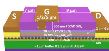
Contact information:Prof.ZHANG Baoshun Suzhou Institute of Nano Tech and Nano Bionics ,Chinese Academy of Science Suzhou,Jiangsu 215123,China. E-mail:bszhang2006@sinano.ac.cn |