Semiconducting single-walled carbon nanotubes (sc-SWCNTs) have attracted considerable attention as one of the most ideal materials for printed thin film transistors (TFTs) and circuits due to their high mobility, solution process, chemical and physical stability and low post-treatment temperature. In the last few years, Printable Electronics Research Center (PERC) at Suzhou Institute of Nano-tech and Nano-bionics has been focusing on developing high-quality printable sc-SWCNT inks and fabricating high-performance flexible printed TFTs and circuits, such as OLED driving circuits, logic gates and circuits.
Recently,a new semiconducting copolymer (named P-DPPb5T) was designed and synthesized with a special nonlinear structure and more condensed conjugation surfaces, which can separate large diameter sc-SWCNTs from arc discharge SWCNTs with high selectivity to the sc-SWCNTs with specific chirality of (14,7), (12,7), (15,5), (16,2), (18,4) and/or (17,6). Printed TFTs based on the sorted sc-SWCNTs ink showed good uniformity, low operating voltage (±2V) and subthrehold swing (SS) (122-161 mV/dec), high effective mobility (up to 17.6-37.7 cm2V-1 s-1) and high on/off ratio (104-107). With the printed TFTs, a CMOS inverter was constructed, which is based on p-type TFT and ambipolar TFT instead of conventional p-type and n-type TFTs. Compared with other recently reported inverters fabricated by printing, the printed CMOS inverters demonstrated better noise margin (74% 1/2 Vdd) and hysteresis free. The inverter has a voltage gain up to 16 at applied voltage of only 1V and low static power consumption. This work has been recently published in Nanoscale, 2016, 8, 4588-4598. Work is underway at PERC to construct backplane driving electronics for flat panel displays and high-performance logic gates and circuits based on printed SWCNT TFTs.
This work was supported by Natural Science Foundation of China (91123034, 61102046), Strategic Priority Research Program of the Chinese Academy of Science (XDA09020201), the Knowledge Innovation Programme of the Chinese Academy of Sciences (KJCX2-EW-M02) and Basic Research Programme of Jiangsu Province (BK2011364 ).
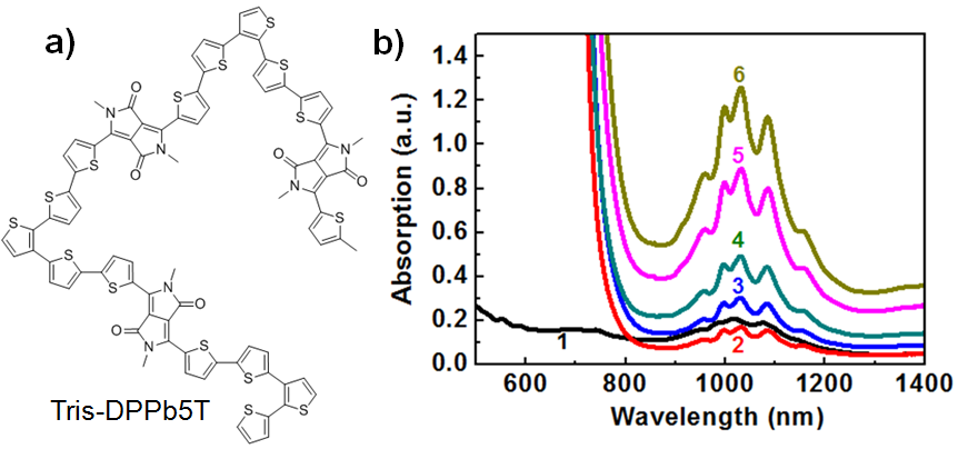
Figure 1. a) Conjugated backbone of P-DPPb5T with three repeating units; b) The UV-Vis-NIR adsorption spectra of arc discharge SWCNTs with different weight ratios of SWCNTs to P-DPPb5T in toluene (20 mL) after centrifugation. (Image by PERC,SINANO)
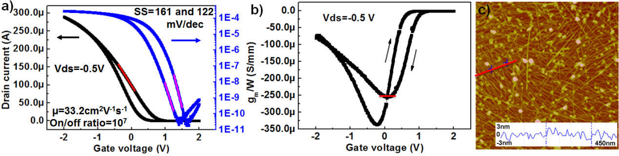
Figure 2. a) Typical transfer curves and transconductance (normalized by the device width, gm/W) of printed bottom-gate TFT on HfO2 substrates and c) AFM image of SWCNT thin film in the device channel (the scale bar in Figure 2c represents 450 nm). (The channel length and width are 20 and 600 μm, respectively.(Image by PERC,SINANO)
Contant information:
Suzhou Institute of Nano Tech and Nano Bionics ,Chinese Academy of Science
Suzhou,Jiangsu 215125,China.
E-mail:jwzhao2011@sinano.ac.cn


