“Hot spot” (HS) as a kind of highly active site is usually composed of some unique units, such as defect, interface, catalyst particle and special structure. For example, Pt, Au, Pd nanoparticles are usually deposited on 1D nanomaterials as “hot spots” to realized certain functions like photo-catalysis and water splitting. Hence, “hot spot” widely exists in photo-(photoelectro-)chemistry, electrochemistry, catalysis etc. Although “hot spot” usually has a small population, it can dominate the behaviour of the whole nanomaterial, and determine the performance. In order to obtain more scientific insights and better applications, it’s necessary to know the growth and working mechanism of the “hot spot”. Ideally, the highly effective way is to study the mechanism at the single nanoparticle level.
To identify these hot spots, Prof. ZHOU Xiaochun and his team at Suzhou Institute of Nano-Tech and Nano-Bionics, Chinese Academy of Sciences (SINANO), study a model system, i.e. “hot spots” on a single Ag nanowire during a galvanic replacement reaction (GRR) by using dark-field microscopy (DFM). Since Ag and Au are plasmatic materials, they are suitable for the optical probing at the single nanoparticle level. GRR between Ag and HAuCl4 are shows as (1) and (2).
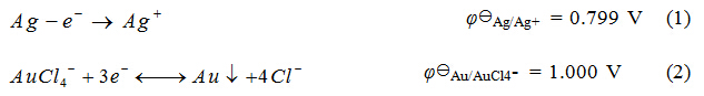

Figure 1. Growth of “hot spots” on single Ag nanowires during GRR in 0.02 mM HAuCl4. (A) Schematic of DFM and a micro-fluidic reactor to image the growth of “hot spots” in GRR. (B)-(C) Dark-field images of many single Ag nanowires in the GRR at the time 0 ks (B) and 2.4 ks (C). (D)-(E) Scattering intensity of nanowire as pointed by arrows in (B) and (C).(Image by SINANO)
We found that the GRR between Ag nanowire and HAuCl4 generate formation of large Ag nanotubes (hot spots) rather than Au on the Ag nanowire. This is an exotic phenomenon since based the principle of galvanic replacement reaction and results reported by others only Au was expected to be reduced and deposited evenly on the surface of Au nanowire. The measurement of open circuit potential (OCP) shows the OCP can drop to ~0.7 V, which is lower than the reduction potential of Ag+. So Ag+ could be reduced to metal Ag cluster. It indicate that the formation of the Ag nanocube induced by the generation of Ag+ and net electrons during GRR at a stage with rapid reaction During GRR. We also measured the distance between adjacent “hot spots”, The appearance of “hot spots” along a single Ag nanowire is a random process The distribution of the hot spots obeys the energy saving principle. An electric double layer was proposed to explain the interactions between the net electrons and Ag+. The surface charges on single Ag nanowire could interact with each other or with other charged objects through an “tunnel”. The study reveals the functions of electric charge at the single nanoparticle level.
The work was published innanoscle,2016,8,12029-12034. This work was supported by the National Natural Science Foundation of China.
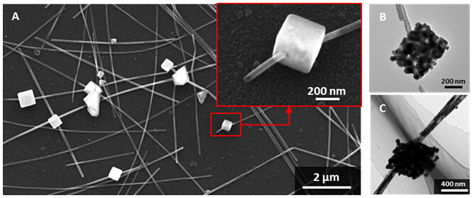
Figure 2. SEM and TEM characterization of “hot spots” on Ag nanowire. (A) SEM image of many Ag nanowires after GRR. (B)-(C) TEM images of “hot spots”.(Image by SINANO)
Contact information: Prof. ZHOU Xiaochun
Suzhou Institute of Nano-Tech and Nano-Bionics, Chinese Academy of Science
Suzhou, Jiangsu 215123, China.
E-mail: xczhou2013@sinano.ac.cn


