|
|
| Picoscale Precision though Ultrathin Film Piezoelectricity |

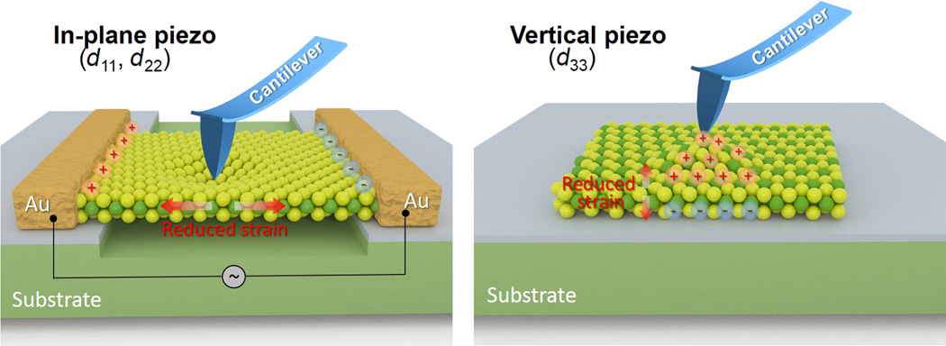
Fig. 1. Schematic illustration of local characterization of in-plane piezoelectricity and vertical piezoelectricity. In-plane piezoelectricity (piezo) (d11, d22) of ultrathin materials is the planar electromechanical couple behavior, where the applied stress and produced piezoelectric potential are located at the in-plane of exposed lattice plane. Vertical piezoelectricity (d33) focus on electromechanical interaction occurred in the vertical axis, which is perpendicular to the surface of materials. The high-precision deformation actuator can be implemented using accurate positioning of the materials surface by vertical inverse piezoelectricity. Credit: X. Wang, X. He, H. Zhu, L. Sun, W. Fu, X. Wang, L. C. Hoong, H. Wang, Q. Zeng, W. Zhao, J. Wei, Z. Jin, Z. Shen, J. Liu, T. Zhang, Z. Liu, Subatomic deformation driven by vertical piezoelectricity from CdS ultrathin films. Sci. Adv. 2, e1600209 (2016). Copyright © 2016 The Authors, some rights reserved; exclusive licensee American Association for the Advancement of Science. Distributed under a Creative Commons Attribution NonCommercial License 4.0 (CC BY-NC). DOI:10.1126/sciadv.1600209. Piezoelectricity (aka the piezoelectric effect) occurs within certain materials – crystals (notably quartz), some ceramics, bone, DNA, and a number of proteins – when the application of mechanical stress or vibration generates electric charge or alternating current (AC) voltage, respectively. (Conversely, piezoelectric materials can vibrate when AC voltage is applied to them.) The piezoelectric effect has a significant range of uses, including sound production and detection, generation of high voltages and electronic frequencies, atomic resolution imaging technologies (e.g., scanning tunneling and atomic force microscopy), and actuators for highly accurate positioning of nanoscale objects – the last being crucial for fundamental research and industrial applications. That being said, subatomic scale positioning still presents a number of challenge. Recently, however, researchers at Nanyang Technological University, Singapore, Chinese Academy of Sciences, Suzhou, and Duke University, Durham demonstrated vertical piezoelectricity at the atomic scale (three to five space lattices) using ultrathin cadmium sulfide (CdS) films. The researchers determined a vertical piezoelectric coefficient (d33) three times that of bulk CdS using in situ scanning Kelvin force microscopy and single and dual ac resonance tracking piezoelectric force microscopy, leading them to conclude that their findings have a number of critical roles in the design of next-generation sensors and microelectromechanical devices. Prof. Zheng Liu discussed the paper that he, Dr. Ting Zhang and their colleagues published in Science Advances, describing a series of challenges they faced starting with using chemical vapor deposition to synthesize 2~3 nm cadmium sulfide (CdS) thin films. "The vertical piezoelectricity, or d33, is the key parameter in piezoelectric materials for the fabrication of actuators used to position objects with extreme accuracy – down to the atomic scale in a broad range of cutting-edge equipment such as atomic force microscopy and scanning tunneling microscopy," Liu tells Phys.org. "Moreover, high-performance ultrathin piezoelectric materials are crucial for the constructing ultra-high resolution and flexible electromechanically coupled devices." Prior to this study, Liu points out, only a few studies reported the synthesis of atomic thin piezoelectric materials by a wet chemical method, examples of which include CdS and cadmium selenide (CdSe) nanoplatelets. "It's a significant challenge to produce high-quality and atom-thin piezoelectric materials," he adds. "In this research, the main challenge in synthesizing ultrathin piezoelectric CdS films via chemical vapor deposition" (or CVD) "lays in the selection of precursors and how to optimize the reaction parameters, such as growing temperature and time." The scientists were then faced with demonstrating d33 vertical piezoelectricity at the atomic scale using ultrathin cadmium sulfide thin films. "When the thickness of materials reaches the nanoscale level," Liu explains, "it's very difficult to verify the piezoelectric effect and determine its values because of the coupling effect from the substrate – and surface geometries may affect the measurements at atomic limits as well." For example, he illustrates, sample surface roughness reaches tens of picometers, which is the same scale with the vertical electromechanical response for materials. 
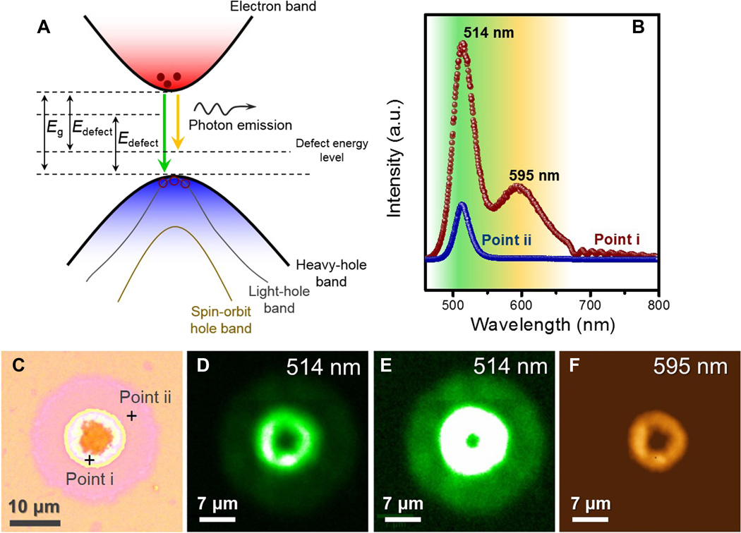
Fig. 2. Spectroscopic characterization of CdS thin film. (A) Energy (E) band structure in the vicinity of the Γ-point of the Brillouin zone, showing the photon emission process. (B and C) PL spectrum of CdS thin film from points i and ii marked in (C) with plus signs, showing strong band edge emission (506 nm) of CdS ultrathin film and defect-related emission (595 nm). (C) Optical image of CdS thin film with a rounded microparticle at its center. a.u., arbitrary units. (D and E) PL mapping at an emission of 514 nm with a different scale bar, demonstrating high uniformity and homogeneity of CdS thin films at the outside area. (F) PL mapping at the 595-nm emission, indicating that the defect-related emission only occurs at the thicker CdS microparticle. Credit: X. Wang, X. He, H. Zhu, L. Sun, W. Fu, X. Wang, L. C. Hoong, H. Wang, Q. Zeng, W. Zhao, J. Wei, Z. Jin, Z. Shen, J. Liu, T. Zhang, Z. Liu, Subatomic deformation driven by vertical piezoelectricity from CdS ultrathin films. Sci. Adv. 2, e1600209 (2016). Copyright © 2016 The Authors, some rights reserved; exclusive licensee American Association for the Advancement of Science. Distributed under a Creative Commons Attribution NonCommercial License 4.0 (CC BY-NC). DOI:10.1126/sciadv.1600209. Lastly – and reminiscent of the challenge in demonstrating d33 vertical piezoelectricity at the atomic scale using CdS thin films – the researchers had to determine the CdS film vertical piezoelectric coefficient with in situ scanning Kelvin force microscopy (SKFM) and single and dual AC resonance tracking piezoelectric force microscopy (DART-PFM). "The quality of ultrathin piezoelectric CdS is the key to obtaining a reliable vertical piezoelectric coefficient." Liu notes. "Some characterization tools like Raman and photoluminescence spectroscopies can help us to identify the CdS sample and confirm its high quality. Also, because of the geometrical vibrations of the CdS samples, the atomic force microscopy characterization should be carefully carried out in order to make sure our conclusions are solid." This required the researchers to examine many SKFM and DART-PFM samples using to reach a solid conclusion about vertical piezoelectric behavior in CdS ultrathin films. Liu comments that addressing these challenges required innovative techniques. "For the first time, we successfully synthesized high-quality atomic thin CdS films using CVD, and we demonstrated vertical piezoelectricity of these films at the atomic scale of 3~5 space lattices" (a space, or crystal, lattice being a periodically repeating two- or three-dimensional array of points or particles) "and observed the vertical piezoelectric domains. More importantly," Liu continues, "our work shows an enhanced vertical piezoelectricity in CdS ultrathin films at a level three times larger than the CdS bulk counterpart, as well as higher than most of traditional piezoelectric materials." These results imply non-trivial piezoelectric behavior at atomic limits for a certain class of materials – which has not yet been well explored – and inspires the search for two-dimensional free-standing layered piezoelectric materials that are only one atom thick. Liu points out that their findings shed light on the design of next-generation sensors, actuators and microelectromechanical devices, in that piezoelectric materials are the most important component for such devices. Specifically, he says that their findings provide the opportunity for next-generation sensors and microelectromechanical devices in three ways: - Flexibility: Ultrathin piezoelectric material materials are naturally like two-dimensional materials in being flexible, allowing them to be conformably used for more complicated electromechanical devices.
- Miniaturization: Ultrathin piezoelectric material materials are a perfect candidate for the fabrication of reduced size, highly integrated devices, especially for mobile phone and wearable devices.
- Inspiration: The study's results will inspire the development of other ultrathin piezoelectric materials, especially two-dimensional piezoelectric materials.

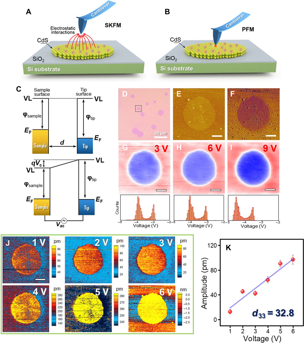
Fig. 3. Noncontact SKFM and standard contact PFM investigation for CdS thin film. (A and B) Schematic illustration of SKFM (A) and PFM (B) measurements. (C) Band diagram of tip and sample when they are electrically separated (top graph) and electrically contacted (bottom graph). d, distance; VL, vacuum levels; q, electronic charge; Vc, contact potential difference. (D) Optical image of CdS thin films. (E and F) Topography (E) and phase (F) images observed by SKFM mode for the single CdS thin film marked in (D). (G to I) Corresponding potential mappings with tip voltages of 3, 6, and 9 V, respectively. Insets show histograms of the surface potential distributions. The CdS ultrathin film has a higher positive voltage (~0.9 V) than the substrate, demonstrating that a large amount of charges are accumulated at a CdS thin film after contact PFM scanning. (J) Amplitude images observed by contact PFM technology with tip voltages from 1 to 6 V, showing remarkable inverse piezoelectricity. (K) Average amplitude variations versus applied voltages calculated from (J). Error bars indicate 1 SD. Scale bars, 2 μm (E to J). The linearly fitted line shows that the measured piezoelectric coefficient deff is ~16.4 pm·V-1, whereas the vertical piezoelectric coefficient d33 is ~32.8 pm·V-1. Credit: X. Wang, X. He, H. Zhu, L. Sun, W. Fu, X. Wang, L. C. Hoong, H. Wang, Q. Zeng, W. Zhao, J. Wei, Z. Jin, Z. Shen, J. Liu, T. Zhang, Z. Liu, Subatomic deformation driven by vertical piezoelectricity from CdS ultrathin films. Sci. Adv. 2, e1600209 (2016). Copyright © 2016 The Authors, some rights reserved; exclusive licensee American Association for the Advancement of Science. Distributed under a Creative Commons Attribution NonCommercial License 4.0 (CC BY-NC). DOI:10.1126/sciadv.1600209. Liu illustrates these points by listing potential examples of such devices – for example, atomically thin piezoelectric devices – and their applications. "For instance, using CdS ultrathin films, the most accurate probe or stage ever fabricated may be achievable, allowing researchers and engineers to manipulate atoms or position tips in atomic force, scanning electron and transmission electron microscopy. In other words, CdS ultrathin films will extend our capability to see and manipulate our world in an extreme way." Of more importance, he adds, such ultrathin piezoelectric devices can be integrated into equipment like autocollimators and Michelson interferometers used in, for example, cold atom studies, the verification of the gravitational inverse square law at short range, and even the detection of gravitational waves. The study also reports the in situ measurement of the ultrathin CdS film vertical piezoelectric coefficient d33, determining the film coefficient to be approximately three times larger than that of bulk CdS. "This value is pretty big for atomically thin materials," Liu explains. "It means that we can get a large voltage change when small pressure or deformation is applied. This makes the material a great candidate constructing sensitive and ultrathin mechanical sensors." 
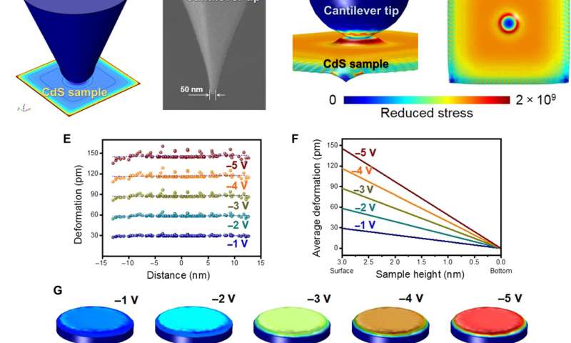
Fig. 4. Simulation of vertical piezoelectricity and subatomic deformation actuator. (A) Three-dimensional image of potential drop on CdS film. (B) Scanning electron microscopy image of a conductive tip for PFM characterization. (C and D) Bottom and side views of stress distribution on CdS film. (E to G) Simulation for subatomic deformation actuator. Different potentials were applied to surface deformation curves (E), mappings (G), and vertical deformation (F) of CdS thin films. Credit: X. Wang, X. He, H. Zhu, L. Sun, W. Fu, X. Wang, L. C. Hoong, H. Wang, Q. Zeng, W. Zhao, J. Wei, Z. Jin, Z. Shen, J. Liu, T. Zhang, Z. Liu, Subatomic deformation driven by vertical piezoelectricity from CdS ultrathin films. Sci. Adv. 2, e1600209 (2016). Copyright © 2016 The Authors, some rights reserved; exclusive licensee American Association for the Advancement of Science. Distributed under a Creative Commons Attribution NonCommercial License 4.0 (CC BY-NC). DOI:10.1126/sciadv.1600209. The researchers concluded that contact piezoresponse force microscopy (PFM) – which uses a conductive tip to apply a highly localized electric field that allows imaging and manipulation of piezoelectric ferroelectric materials – could significantly change the surface potential of a CdS ultrathin film by applying stress to its surface. "Typically, applying mechanical stress to a piezoelectric material will generate electric charge that accumulates at the surface of the material, which is how we identify the piezoelectric materials," Liu tells Phys.org. "We therefore believe that this results from piezoelectric polarizations giving rise to a large piezoelectric potential, in turn leading to a remarkable spatial separation of electrons and holes." In this case, electrons generated by the piezoelectric effect will be trapped into the silicon dioxide (SiO2) dielectric layers, while the holes will be trapped inside the crystal boundary of the CdS films. The scientists state that their work may pave a way to the synthesis of ultrathin lattice scale nanomaterials using CVD method, which is a low-cost method for producing high quality samples. In addition, Liu notes, the materials provided by their study will enable the high-integrated and multi-functional devices by simply coating or transferring the film to the device. "For actuator applications, our work will promote next generation actuators with extreme resolution for their potential use in characterization tools such as ultra-high resolution microscopy; for atom manipulation and fabrication; or potentially for the detection of ultra-low deformation in, for example, cold atom studies, verification of the gravitational inverse square law at short range, and even the detection of gravitational waves." Moving forward, Liu says, the scientists will determine the relationship between the vertical piezoelectric coefficient d33 and the thickness of CdS at atomic scales. "Well also synthesize other piezoelectric, ferroelectric and layered piezoelectric/ferroelectric ultrathin materials, and explore their electromechanical properties." Based on this material and micro/nano-manufacture technology, the researchers hope to design and fabricate next-generation actuators for accurate positioning of minute objects, such as nanoparticles at subatomic scales, using their novel materials. In addition, the large vertical piezoelectric coefficient d33 makes this material promising to construction of ultrathin and sensitive pressure sensors for detecting miniscule forces. If the low detection limit of sensor reaches to nanoscale levels, the device could monitor single biological cell migration. "Our study will inspire material scientists to hunt for other non-trivial ultrathin or layered piezoelectric or ferroelectric materials," Liu tells Phys.org. "Engineers can employ our CdS ultrathin films to design and fabricate novel microelectromechanical systems," or MEMS, "and nanoelectromechanical systems," or NEMS, "with high-integration and multi-functionalities, and may benefit when developing cutting-edge scientific instruments. Furthermore," he concludes, "novel and flexible consumer electronic devices can be developed based on our study." (Phys.org) Reference: Subatomic deformation driven by vertical piezoelectricity from CdS ultrathin films. Contact Information: ZHANG Ting International Laboratory for Adaptive Bio-nanotechnology (i-Lab), Suzhou Institute of Nano-Tech and Nano-Bionics E-mail: tzhang2009@sinano.ac.cn |
|

