Recently, Prof. WANG Rongxin’s group, at Suzhou Institute of Nano-tech and Nano-bionics, Chinese Academy of Sciences, observed interesting enhancement effect of transparent conductive nanocrystalline oxide thin layer on performance of UV detectors fabricated on GaN. Experimental results show that the optical responsivity of the detectors can be significantly influenced by a thin layer of nanocrystalline GZO.
Metallic materials are common in the fabrication of electrodes for UV PD structures. For the Au/Ni/GaN device, efficient photo absorption occurs only in the GaN substrate. The UV PDs show a sharp cut-off response at around 365 nm wavelength in correspondence to the band edge of GaN. However, as opaque metal electrodes block more light, transparent conductive electrodes could be used to obtain higher efficiency of optical to electrical conversion in PDs. When a layer of GZO is as transparent electrode materials, Wang’s team found novel and interesting phenomenon, i.e., spectral response became much broader, especially extraordinary enhanced deep-UV photoresponse at around 250 nm appears in the solar blind spectral zone as shown in Figure 1 (a). It is because efficient photo absorption can occur in both GaN substrate and the GZO contact thin film layer whose strong photo absorption take place in the solar blind spectral zone as shown in figure 1 (b).
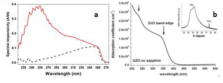
Figure1. (a)Measured spectral responsivity curves of Au/Ni/GaN (black dashed line) and GZO/GaN (red solid line) photodetectors. (b)The absorption coefficient of the GZO film sputtered on sapphire vs. the wavelength. The inset shows the XRD patterns of the film(Image by SINANO).
To achieve higher performance of UV detectors, great progress and structures have been achieving and considering by many researchers. Prof. Wang’s team investigated a structure with transparent conductance oxide layer. When a layer of GZO is inserted between metal electrode and Fe-doped GaN epilayer, optical responsivity of the PDs was significantly improved (i.e., 100-fold). TEM image of the interface between GZO thin film and GaN shows that the whole GZO contact layer consists of a 4 nm amorphous bottom layer and a nanocrystalline top layer containing a lots of grains with size of several nanometers. That formation of oxides and hydroxides layer would alter the Schottky-Mott barrier height and ideality factor. Obviously, the GZO insertion layer plays a decisive role in the great enhancement of optical responsivity of the Fe-doped GaN PDs. Valence-band discontinuities across the GZO-GaN interface, extrinsic doping effect of GZO and Fe-doped GaN are argued to be responsible for the great enhancement of the device responsivity. Inserting a transparent oxide conducting layer could be an effective method to improve performance of GaN based UV PDs.
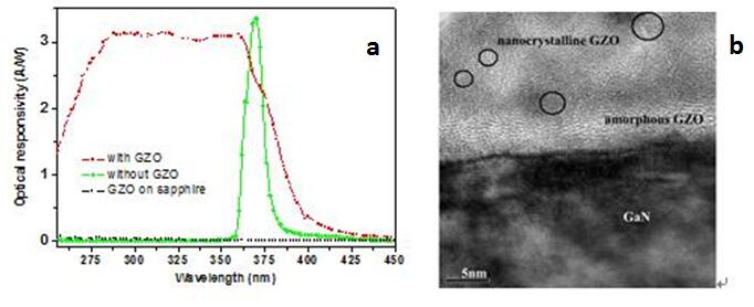
Figure2. (a) The measured spectral responsivities of the PDs at room temperature. The red square line represents the spectral responsivity of the PD with an insertion layer of GZO while the green rhombus line is for the PD. (b) Cross-sectional TEM image of GZO thin film on GaN. Nanocrystals (circled regions) can be clearly resolved in the GZO thin film(Image by SINANO).
Journal Reference:
1).R. X. Wang*, L. C. Yang, Y. M. Zhang, K. Fu, S. J. Xu, J. F. Wang, K. Xu, B. S. Zhang, and H. Yang, “The effect of Ga-doped nanocrystalline ZnO electrode on deep-ultraviolet enhanced GaN photodetector”, Applied Physics Letters, 102, 212104 (2013) http://aip.scitation.org/doi/10.1063/1.4808381.
2). Z. Xing, R.X. Wang*, Y.M. Fan, J.F. Wang, B.S. Zhang, K. Xu “The effect of transparent conductive nanocrystalline oxide thin layer on performance of UV detectors fabricated on Fe-doped GaN”, Materials Science in Semiconductor Processing 57, 132–136 (2017) http://dx.doi.org/10.1016/j.mssp.2016.10.017.
Contact Information:
Prof. WANG Rongxin, Nano-X, Suzhou Institute of Nano-Tech and Nano-Bionics,
Email: rxwang2008@sinano.ac.cn


