Unlike the colors produced by pigments or dyes, the structural colors arise from the physical interaction of light with nanometer scale structures. Depending upon the specific optical effects like scattering, diffraction or interference of the artificial structures, the structural colors can be can be tuned with great degree of freedom. Particularly, color generation by metallic or dielectric based structures is highly resistant to fading and photobleaching, which would be an essential metrics for future displaying or color printing techniques.
The application of metallic nanoparticles in structural coloration can be traced back for centuries, famously exemplified by the Lycurgus Cup. Recent progress in nano-optics and nanotechnology allow us to lift the veil on the tiny metals-mediated coloration. The optical properties of metal nanoparticles are governed by collective oscillations of free electrons, which give rise to amplified scattering cross sections at characteristic frequencies and therefore presenting specific color perceptions from our eye observation.
Plasmonic nanoscatters-mediated colorations have attracted extensive research interests in the past few years. Applications such as sensing, high resolution imaging and display have been proposed and demonstrated. With the trends toward miniaturization and low power consumption, besides their utility in passive spectral filtering, integration of the structural coloration with the photovoltaic light harvesting represents an attractive direction for self-power display, filter-free imaging, and aesthetically pleasing solar cells.
Pioneer approaches for structural colorations rely on the incorporation of scattering elements that are always embedded in or fabricated on low index hosts. However, for the case of highly asymmetric index configurations like the attachment of plasmonic nanoscatters on most commonly used semiconducting substrates, the scattering colors are undermined in both the gamut and efficiency, limiting their utility in various integrated optoelectronic applications.
The team from Suzhou Institute of Nano-Tech and Nano-Bionics, Chinese Academy of Sciences develops a compact multifunctional device that combines the capacities of vivid plasmonic scattering coloration and high efficient photoelectric conversion on a silicon platform. The achievements rely on the spectrally or spatially reshaping of the resonant position and escape cone of the plasmonic scattering waves via an impedance matched plasmonic nanoscatter/silicon configuration. Furthermore, benefiting from the non-resonant and diffraction light trapping effects of the nanoscatters, the devices simultaneously demonstrates vivid colors and comparable photoelectric conversion efficiency against the anti-reflective reference devices. Reflective coloration across the full visible spectrum was achieved together with a power conversion efficiency of 8.3% that is 96-99% of the reference device without nanoscatters, i.e., realizing coloration at a negligible cost of the power conversion efficiency. The integration offers both color-sorting and light-harvesting capabilities with superiorities such as reduced spatial optical crosstalk, improved photoresponsitivity, self-charging, high integrity, and so on in potential applications including advanced display, imaging, and photovoltaics.
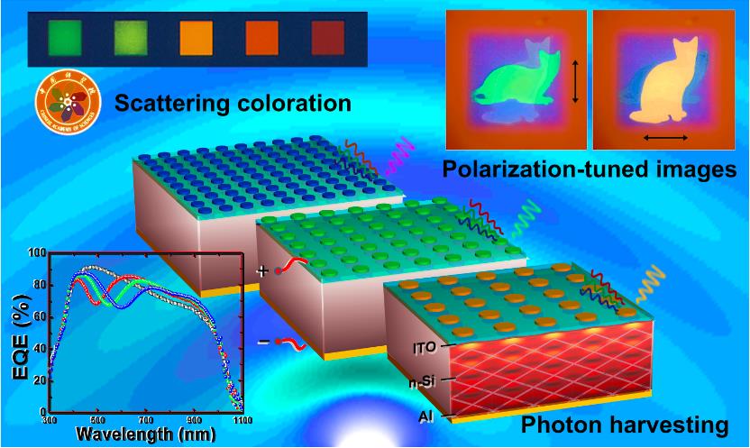
Figure1 Multifunctional Silicon Optoelectronics Integrated with Plasmonic Scattering Color.(Image by SINANO)
Related findings were published in ACS NANO (10:11076, 2016) with title of Multifunctional Silicon Optoelectronics Integrated with Plasmonic Scattering Colors. And the study is sponsored by the grants from the National Natural Science Foundation of China (No. 11274344, 11604367 and 61574158), the key Research and Development Projects, Ministry of Science and Technology (No. 2016YFB0402500), the Cutting-edge Key Research Program of Chinese Academy of Sciences (No. QYZDB-SSW-JSC014), the Natural Science Foundation of Jiangsu Province (NO.BK20150369) and the Suzhou Science and Technology Development Program Foundation (No. SYG201529).
Contact Information:
Prof. CHEN Qin, Suzhou Institute of Nano-Tech and Nano-Bionics, Chinese Academy of Sciences
Email: qchen2012@sinano.ac.cn


