GaN high electron mobility transistors (HEMTs) are promising candidates for future power switching applications, due to their wide band gap, high electron mobility, and high energy conversion efficiency. However, the common AlGaN/GaN HEMTs are naturally normally-on devices, due to the high density two dimensional electron gas (2DEG). For safety reasons, GaN HEMT used in power converters must be normally-off devices.
Several techniques have been proposed to obtain normally-off AlGaN/GaN HEMTs, such as recessed gate, fluorine plasma ion implantation, p-GaN gate and Cascode structure. Among them, p-GaN gate HEMT has been considered as one of the most promising candidates for normally-off devices. In this case, the etching of p-GaN over AlGaN barrier is a very critical step and there are still a lot of challenges, such as etching damage, roughness, uniformity, chamber conditioning, and so on, especially for the large size wafer.
Recently, a team of researchers, led by Prof. ZHANG Baoshun at Suzhou Institute of Nano-Tech and Nano-Bionics (SINANO), Chinese Academy of Sciences, proposed a different method to fabricate this device. Instead of using etching technology, hydrogen plasma was adopted to compensate holes in the p-GaN above the two dimensional electron gas (2DEG) channel to release electrons in the 2DEG channel and form high-resistivity area to reduce leakage current and increase gate control capability. Meanwhile, the high resistivity area works as a surface screening layer which is helpful to mitigate the current collapse.
The fabricated p-GaN/AlGaN/GaN HEMT exhibits normally-off operation with a threshold voltage of 1.75 V, a subthreshold swing of 90 mV/dec, a maximum transconductance of 73.1 mS/mm, an ON/OFF ratio of 107, and a maximum drain current density of 188 mA/mm at a gate bias of 6 V.The study entitled “Normally-off p-GaN/AlGaN/GaN high electron mobility transistors using hydrogen plasma treatment” has been published in Applied Physics Letters.
This research was supported by Key Technologies Support Program of Jiangsu Province and the National Key Scientific Instrument and Equipment Development Projects of China.
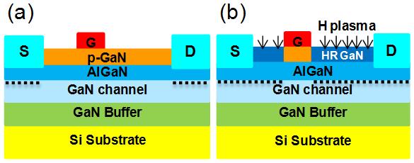
Figure 1. Schematic diagram of devices: (a) before H plasma, (b) after H plasma.(Image by SINANO)
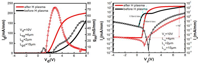
Figure 2. I-V characteristics of devices: before H plasma (black) and after H plasma (red).(Image by SINANO)
Contact Information:
Prof. ZHANG Baoshun, Suzhou Institute of Nano-Tech and Nano-Bionics, Chinese Academy of Sciences
Email: bszhang2006@sinano.ac.cn


