Fabrication of high-performance and environmentally stable n-type single-walled carbon nanotube (SWCNT) transistors by printing and their integration into complementary circuits are widely recognized as key to achieving the full potential of carbon nanotube electronics. A number of methods for the polarity conversion of SWCNT transistor have been reported to date, including chemical doping by active metals and organic reducing reagents, electrostatic doping by metal oxide thin films, and “physicochemical field-effect” doping by silicon nitride. However, it is still a big challenge for achieving high-performance and environmentally stable n-type SWCNT TFTs by printing technology because they are very sensitive to oxygen and water in air.
The Printable Electronics Research Center (PERC), Suzhou Institute of Nano-Tech and Nano-Bionics (SINANO), Chinese Academy of Sciences (CAS), reported a novel approach to selectively and simultaneously constructing p-type and n-type top-gate SWCNT TFTs on a plastic substrate in 2016. CMOS inverters and ring oscillators with improved performance have been demonstrated.
Recently, a much simpler, more efficient, and robust method has been developed for the polarity conversion using cheap and readily available ethanolamine as an electron doping agent. P-type bottom-gate SWCNT TFTs can be selectively converted into n-type by deposition of ethanolamine inks on the transistor active region via aerosol jet printing.
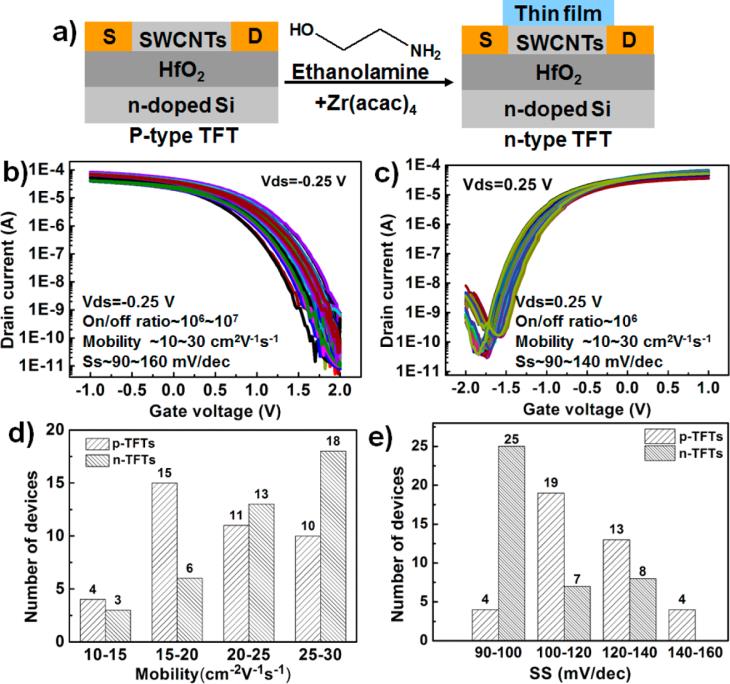
Figure 1 Structures of p-type and n-type TFTs and electrical properties of printed bottom-gate SWCNT TFTs before and after deposition of the polarity conversion inks. (Image by SINANO)
As an example, CMOS inverters were constructed using the printed p-type and n-type TFTs and they exhibited a large noise margins of 50% and 103% of 1/2 Vdd = 1 V and a voltage gain as high as 30 (at Vdd = 1 V) as shown in Figure 2. Additionally, the CMOS inverters show full rail-to-rail output voltage swing and low power dissipation (0.1 μW at Vdd = 1 V). The new method paves the way to construct fully functional complex CMOS circuitry by printed SWCNT TFTs.
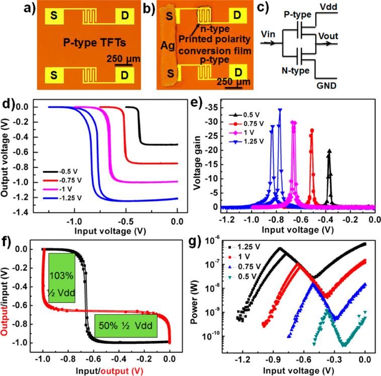
Figure 2 Performance of a CMOS inverter based on printed p-type and n-type SWCNT TFTs.(Image by SINANO)
Contact Information:
Prof.ZHAO Jianwen, Suzhou Institute of Nano-Tech and Nano-Bionics, Chinese Academy of Sciences
Email: jwzhao2011@sinano.ac.cn
Reference:Flexible CMOS-Like Circuits Based on Printed P-Type and N-Type Carbon Nanotube Thin-Film Transistors
Selective Conversion from p-Type to n-Type of Printed Bottom-Gate Carbon Nanotube Thin-Film Transistors and Application in Complementary Metal–Oxide–Semiconductor Inverters


