|
|
| Scientists Fabricate High-performance AlGaN/GaN MIS-HEMTs Using In-Situ Pre-Deposition Plasma Nitridation and LPCVD-Si3N4 Gate Insulator |
GaN power transistors are widely investigated because of their high breakdown voltage, low on-state resistance and fast switching speed. Conventional AlGaN/GaN Schottky high electron mobility transistors (HEMTs) suffer from a high gate leakage and a small gate swing. By inserting an insulator under gate metal, the MIS-HEMTs are highly preferred over the Schottky-gate HEMTs for high-voltage power switches, owing to the suppressed gate leakage and enlarged gate swing. However, the insertion of the gate dielectric creates an additional dielectric/(Al)GaN interface that presents some great challenges to AlGaN/GaN MIS-HEMTs, such as the threshold voltage (Vth) hysteresis, current collapse and the reliability of the devices. Recently, Prof. ZHANG Baoshun’s group, at Suzhou Institute of Nano-tech and Nano-bionics, Chinese Academy of Sciences presents a fabrication technology of high performance AlGaN/GaN metal-insulator-semiconductor high electron-mobility transistors (MIS-HEMTs) using in-situ pre-deposition plasma nitridation and LPCVD-Si3N4 gate insulator. The in-situ pre-deposition plasma nitridation process improves the LPCVD-Si3N4/GaN interface quality by removing oxygen-related bonds and reducing surface dangling bonds. A high-quality LPCVD-Si3N4/GaN-cap interface has been obtained. The fabricated MIS-HEMTs exhibit a very-low Vth hysteresis of 186 mV at VG-sweep = (-30 V, +24 V), a high breakdown voltage of 881 V with the substrate grounded. Switching after an off-state VDS stress of 600 V, the dynamic on-resistance Ron is only 18% larger than the static Ron. Thus, the LPCVD-Si3N4/GaN/AlGaN/GaN MIS-HEMT processed with in-situ pre-deposition plasma nitridation exhibits promising characteristics for power electronic applications.This work has been published in the journal IEEE Electron Device Letters, 2017, 38, 236.This work was partly supported by the Key Technologies Support Program of Jiangsu Province (grant No. BE2013002-2), National Natural Science Foundation of China (61306100) and the National Key Scientific Instrument and Equipment Development Projects of China (2013YQ470767), And the authors are grateful for the technical support provided by Nanofabrication Facility and Platform for Characterization and Test of SINANO, Chinese Academy of Science. 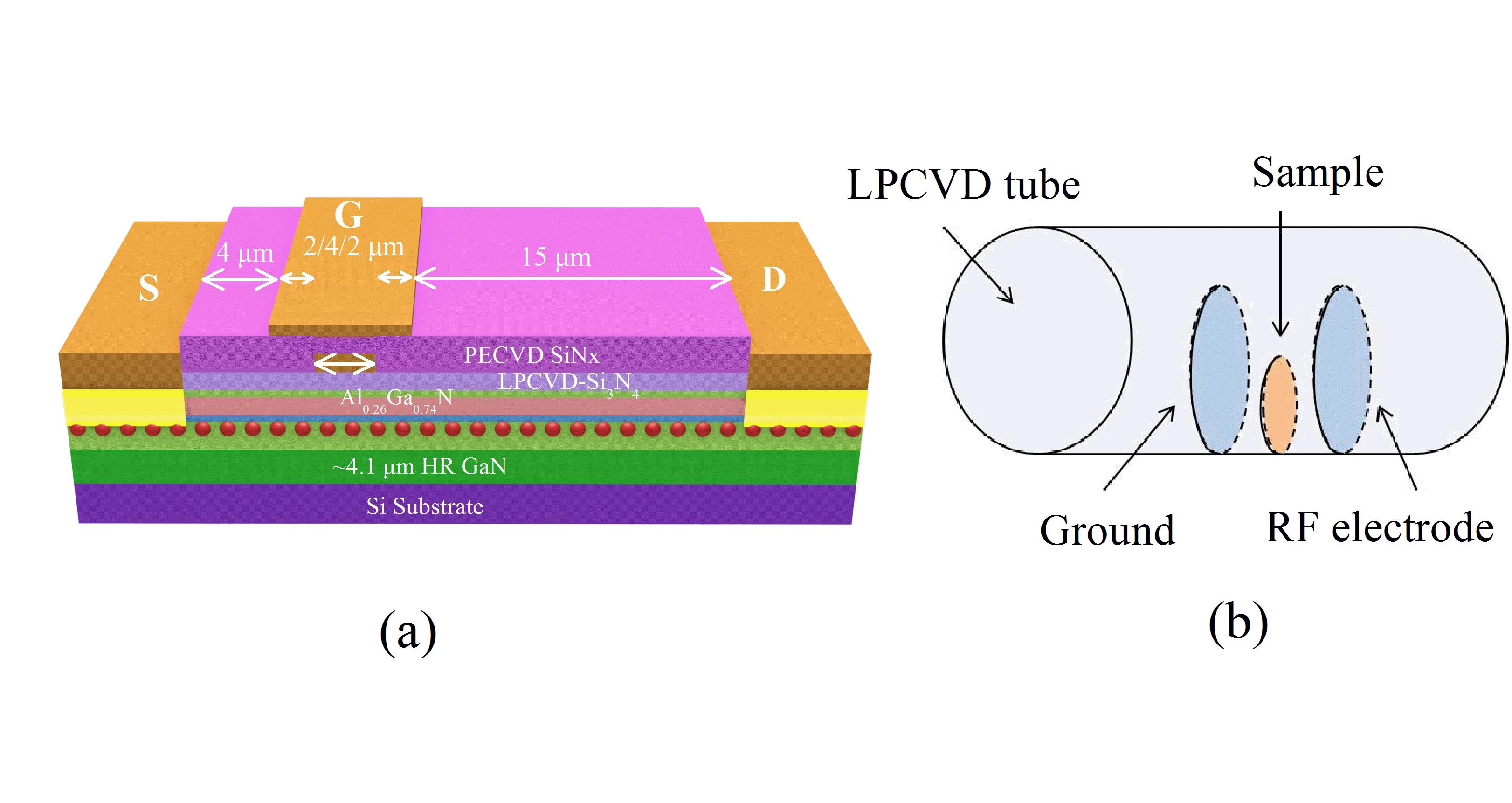
Figure.(a) Schematic of AlGaN/GaN MIS-HEMTs with 20 nm LPCVD-Si3N4 as a gate dielectric and (b) a reformed LPCVD system.(Image by SINANO) Contact Information: Prof. ZHANG Baoshun, Suzhou Institute of Nano-Tech and Nano-Bionics, Chinese Academy of Sciences Email: bszhang2006@sinano.ac.cn |
|


