Chemical vapor deposition (CVD) growth of high-quality graphene has emerged as the most promising technique in terms of its integrated manufacturing. Through last decade’s efforts (2007-2017), numerous breakthroughs have been made in the areas of fast growth, high quality and mass production by CVD growth of graphene on Cu foils. However, it is still a challenge to realize high quality and large quantity of graphene films at a fast growth rate simultaneously, regardless of roll-to-roll (R2R) or batch-to-batch (B2B) methods. Several reasons account for this problem. Firstly, the mismatch between Cu substrate and graphene leads to high density of grain boundaries, degrading the physical properties of graphene; Secondly, in order to suppress the nucleation sites, traditional CVD techniques usually decrease the feedstock concentration, which results in a rather low growth rate, typically between 0.03 μm/s and 0.36 μm/s. Thirdly, with enlargement of Cu foil size, the growth atmosphere is strongly affected by the flow resistance, making the graphene films nonuniform or discontinuous in mass production.
The research groups of professor LIU liwei at Suzhou Institute of Nano-Tech and Nano-Bionics (SINANO), Chinese Academy of Sciences, cooperated with the researchers in Suzhou Graphene Nanotechnology Co., Ltd, launched a systematic and in-depth study on this issue. Firstly, they study the roles of O2 and H2 in crystal orientation transition of Cu foils. Their work shows that the Cu2O layer on Cu surface tends to stabilize the Cu(001) orientation during annealing process. After removing the oxide layer by introducing H2, the Cu(001) orientation can completely changes into Cu(111) orientation(Figure. 1). The density functional theory (DFT) calculations further reveal the mechanism of transition(Figure. 2). This work can be helpful for revealing the roles of O2 and H2 in controlling the formation of Cu monocrystal substrate as well as in growing high-quality graphene films. The related work has been published on the journal of Scientific Reports.7, 45358 (2017).
Based on the above work, they further developed a stationary-atmospheric pressure CVD (SAPCVD) system based on thermal molecular movement, which enables fast B2B growth of continuous and uniform graphene films on 20 pieces of stacked Cu(111) foils with a growth rate of 1.5 μm/s. The monolayer graphene of batch production is found to nucleate from arrays of well-aligned domains, and the films possess few defects and exhibit the high carrier mobility up to 6944 cm2/Vs at room temperature(Figure. 3).
Compared with traditional low-pressure CVD (LPCVD) or atmospheric-pressure CVD(APCVD) system, the advantages of SAPCVD system are mainly embodied in the following three points. Firstly, the growth gases of SAPCVD is free of the flow resistance due to its stationary atmosphere, which conduces to the mass production of graphene; Secondly, the SAPCVD system can realize single layer graphene with a 1500% change of carbon concentration, which is advantageous for uniform graphene growth; Thirdly, the carbon source in SAPCVD system can be fully decomposed, meanwhile, SAPCVD can also decrease the use of vacuum equipment, lowering the cost of graphene growth. The results indicate that the stationary-atmospheric pressure CVD system combined with single domain Cu(111) substrates makes it possible to realize fast batch synthesis of high-quality graphene films, which open up enormous opportunities to use this unique 2D material for industrial device applications. The related work has been published in the journal of Small (DOI: 10.1002/smll.201700651).
The series of work was supported by the National Natural Science Foundation of China, the projects of Jiangsu province and Suzhou city.
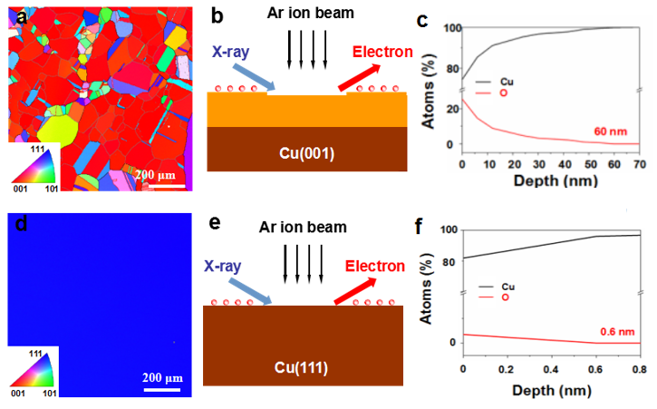
Figure1.Manipulation of Cu orientation by Ar and H2. (a,d) EBSD orientation maps of Cu foils annealed under Ar and H2; (b,e) Schematic structures for the XPS depth-profiling; (c,f) Relative atomic contents of O and Cu as a function of etching depth.(Image by SINANO)
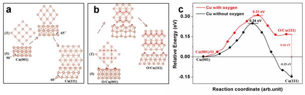
Figure.2. DFT calculations of the effect of oxygen on the orientation transition from Cu(001) to Cu(111).(Image by SINANO)
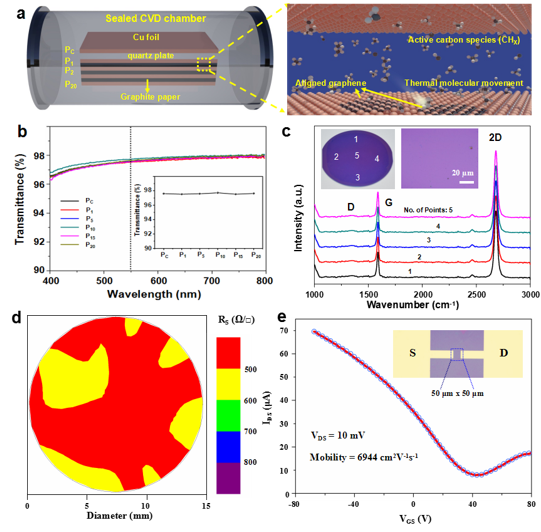
Figure.3. Batch to batch production of graphene films on stacked Cu foils by SAPCVD system. (a) Schematic diagram of growth of graphene films in a sealed CVD chamber; (b) UV-vis spectra of the transferred graphene films on glasses; (c) Raman spectra of graphene film with five typical points across the 2 inch SiO2/Si; (d) Sheet resistance distribution of the monolayer graphene film; (d) Drain current versus gate voltage for the graphene field-effect-transistor measured at room temperature.(Image by SINANO)
Reference: https://www.nature.com/articles/srep45358
http://onlinelibrary.wiley.com/doi/10.1002/smll.201700651/full
Contact Information:
Prof. Liu Liwei, Suzhou Institute of Nano-Tech and Nano-Bionics, Chinese Academy of Sciences
Email: lwliu2007@sinano.ac.cn
Website of Liu Liwei's group: http://nanodevices.sinano.ac.cn/nami/index.php?tid=316


