Atomically thin black phosphorous (BP), a novel 2D semiconductor material, has a thickness-dependent direct bandgap from 0.3 eV for bulk to 1.5 eV for monolayer, which provides a bridge to fill the energy gap between graphene and TMDCs. Few-layer BP FETs have been demonstrated with a high mobility (>1000 cm2/Vs) and on/off current ratio (~105).The tunable bandgap characteristic of BP coupled with its high mobility excites the semiconductor industry and expected as a good candidate for high-performance nanoelectronics. However, pristine BP is p-type and exhibits strong asymmetry between electron and hole transport, where both the electron current and mobility are several orders of magnitude lower than that of holes. The unipolar characteristic of BP makes it difficult to accomplish the complementary devices in a single BP flake. Therefore, an effective electron doping for n-type BP will be necessary and significant to fulfill a large number of practical semiconductor devices, such as logic gates, photodiodes, light emitting diodes, solar cells and so on.
Conventionally, three categories of methods have been widely used to modulate the carrier type of semiconductors, some of which were already applied for the n-doping of BP: i) substitutional doping, including substitutional doping during growth, ion implantation, plasma treating, etc; ii) charge transfer from an electron donor or acceptor, involving gas molecules, metal particles, organics and oxides; iii) field-induced doping. For 2D materials, due to their stable lattice structures and absence of dangling bonds, substitutional doping has been only achieved in very few 2D semiconductor materials. While, the performance of the semiconductor especially its transport property employing this approach will be degraded seriously because of the inevitable defects and charged impurity scattering centers. Surface charge transfer is another effective method to dope 2D materials. However, surface charge may suffer from the disadvantages of unstable as volatile and incompatible to complementary semiconductor routes, which is unsubstantial for practical uses. A promise non-volatile and stable n-doping method is still absent for BP electronics. Silicon nitride (SixNy), which contains a high density of positive charge centers originating from +Si≡N3 dangling bonds known as K+ centers, is generally utilized in Si solar cells to induce a favorable band bending and surface inversion of p-type Si from the field-induced effect. And, this field-induced n-doping scheme could also be available for 2D materials without causing any damage to the lattice nor experiencing a drop in mobility due to ionized impurity scattering, which was demonstrated in the experiments with WSe2 devices. Furthermore, silicon nitride is a CMOS compatible material, which is often used as an insulator and chemical barrier in manufacturing integrated circuits to electrically isolate different structures or as an etch mask in bulk micromachining. It is also a good passivation layer for microchips because of its efficient isolation of water molecules. To date, no study has experimentally demonstrated the use of field-induced effect within silicon nitride to modulate the charge carrier type of BP and apply it for complementary electronic devices.
Professor ZHANG Kai‘s group from Suzhou Institute of Nano-Tech and Nano-Bionics, Chinese Academy of Sciences has been committed to growth and doing on BP, as well as the device fabircation and measurement for several yeras. Previously, they had systematically studied the growth of Selenium doped Black Phosphorus by mineralizer-assisted gas-phase transformation method, and its applications for high-responsivity photodetector and femtosecond laser. Their work were reported in small(2016, 12, 5000–5007)and Journal of Materials Chemistry C (2017, 5, 6129—6135), respectively. Recently, Professor ZHANG Kai collaborated with Professor ZHANG Yuegang from Tsinghua University and Professor ZHANG Han from Shenzhen University, first investigated the field-induced n dope of few-layer BP with the SixNy dielectric coating. The pristine p type BP transfers to n type and electron mobility significantly improved to ~176 cm2/Vs at room temperature. Using this doping approach, planar BP PN diode and logic inverter were realized and demonstrated with excellent performances. This work provides a promising n-dope strategy for BP as well as other 2D semiconductors and paves the way towards high-performance BP-based complementary logic electronics, light-emitting diode, photovoltaic devices, etc. This work has been published in Advanced Functional Materials (DOI: 10.1002/adfm.201702211).
This work is supported by the Hundred Talent Program of Chinese Academy of Sciences, the National Natural Science Foundation of China (11574349) and the Natural Science Foundation of Jiangsu province (BK20150365).
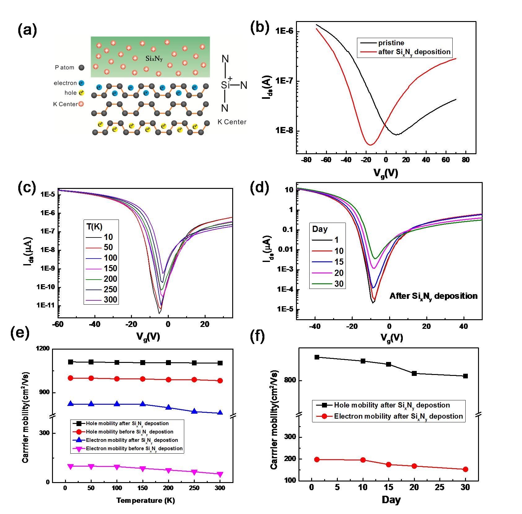
Figure 1. (a) Scheme of the field-induced n-doping of BP with SixNy. (b) Isd–Vg (transfer) characteristics, in logarithmic scale,of the BP FET before (black line) and after (red line) SixNy deposition measured with source-drain voltage of 100 mV. (c) Transfer characteristics of the SixNy n-doped BP FET measured with Vsd of 100 mV at different temperature from 10 to 300 K. (d) Transfer characteristic at room temperature with Vsd of 100 mV for the SixNy n-doped BP FET at different stages undergoing one-month air exposure. (e) Temperature-dependent of the hole and electron mobility of the BP FETbefore and after the modulation of SixNy. (f) Time-dependent of the hole and electron mobility of the SixNy n-doped BP FET at room temperature.
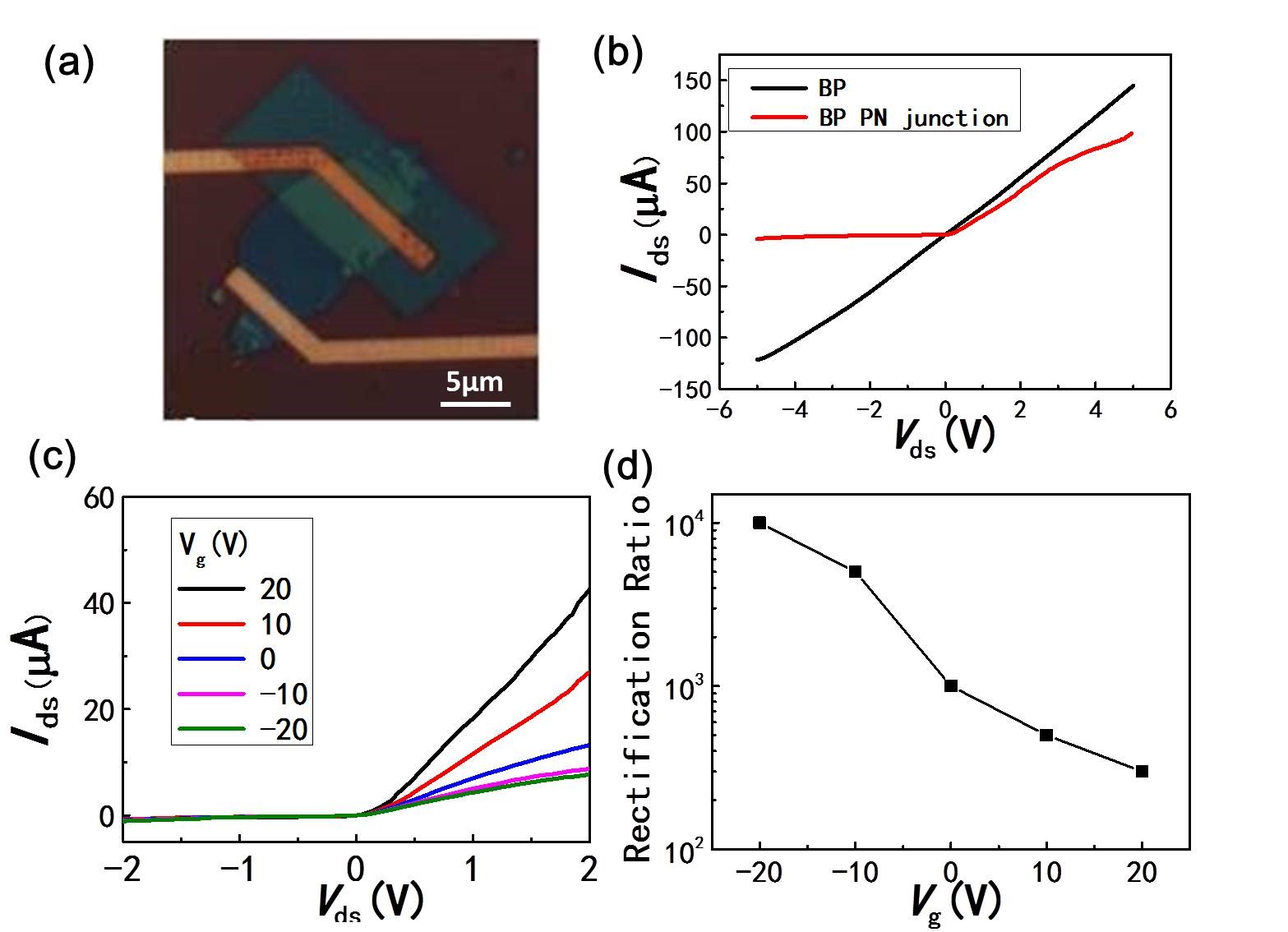
Figure 2.(a) Optical image of a representative BP planar PN diode. The rectangular green panel in the image is the area deposit with SixNy for n-type BP. (b) Output characteristics of the BP FET (black line) and BP PN diode (red line). Typical rectification behavior is shown with the BP PN diode. (c) Gate tunable output characteristics of the BP PN diode under gate voltage modulation in the range of -20 to 20 V. Ids increases as the back gate voltage increases. (d) Rectification ratio as a function of back gate voltage from -20 to 20 V.
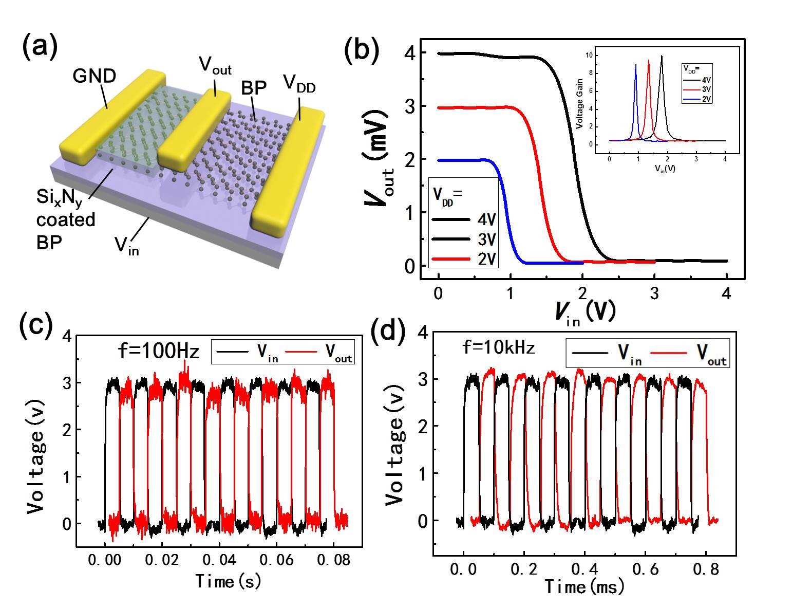
Figure 3.(a) Schematic of the BP logic inverter in using a pristine BP p-FET channel and a SixNy doped BP n-FET channel fabricated on a single sheet of BP flake. (d) Output voltage, Vout, as a function of the input voltage, Vin, at supply voltages, VDD, ranging from 2 to 4 V. The gain of the inverter is shown in the inset. Output voltage, Vout, as a function of the input voltage, Vin, at a frequencyof (c) f = 100Hz and (d) f = 10kHz for the inverter.
Contact Information:
Prof. ZHANG Kai, Suzhou Institute of Nano-Tech and Nano-Bionics, Chinese Academy of Sciences
Email: kzhang2015@sinano.ac.cn
Reference:http://onlinelibrary.wiley.com/doi/10.1002/adfm.201702211/full


