Multi-junction solar cells (SCs) are used for space power generation due to their high conversion efficiency and good radiation resistance. The efficiencies of triple-junction SCs continue to rise in the recent years with the development of material growth and the optimized band gap design. In the case of four or more junctions, the dislocations resulted from metamorphic buffer in the upright lattice-mismatched growth would deteriorate the device performance. Recently, wafer bonding technique was used to integrate lattice-mismatched sub-cells from different substrates into a single device, overcoming the dislocation problems associated with metamorphic growth without both electrical loss and optical loss. The GaInP/GaAs//InGaAsP/InGaAs four-junction (4J) SCs using the technique of wafer-bonding has reached the highest efficiency under concentration. In order to apply this new-type SCs in future space application, the study of radiation effects and proper radiation hardening methods is still necessary. The research on the radiation effects of wafer bonded GaInP/GaAs//InGaAsP/InGaAs 4J SCs has not been reported yet. Recently, Professor LU Shulong and his group from the Suzhou Institute of Nano-Tech and Nano-Bionics (SINANO), Chinese Academy of Sciences (CAS), developed a high radiation hardness wafer-bonded four-junction solar cell grown by MBE. After exposure to 1-MeV electron irradiation at 1×15 e/cm2, an end of life remaining factor of approximately 85% was obtained. The spectral response result showed that the degradation of cell performance was mainly due to the damage on the InGaAsP and InGaAs bottom two sub-cells. Single junction InGaAsP SC has a ralatively better resistance to the electron damage than the InGaAs SC. The relationship of degradation of Voc between sub-cells and the 4J SC indicates a highly radiation resistant bonding interface. We tentatively attributed this behavior to the good device structure design of the 4J SCs. The rigorous demand of current matching in 4J SCs in contrast to 3J SCs increased the reasonability of the thickness design under electron irradiation. The investigation about the damage mechanism and structure optimization will further improve the EOL of the room-temperature wafer bonded four-junction solar cell. In addition, an increased material quality of grown by MBE must be helpful to increase the device performance. 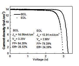
Figure 1 The J-V characteristics of the wafer-bonded four-junction solar cell before (line) and after 1 MeV electron irradiation at 1×10¹⁵ e/cm-2 (dots).(Image by SINANO) 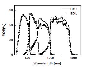
Figure 2 The external quantum efficiency of the wafer-bonded four-junction solar cell before (BOL) and after irradiation with 1 MeV electrons at a fluence of 1×10¹⁵ e/cm-2.(Image by SINANO) Contact Information: Prof.LU Shulong, Suzhou Institute of Nano-Tech and Nano-Bionics, Chinese Academy of Sciences
Email: sllu2008@sinano.ac.cn Reference:http://www.sciencedirect.com/science/article/pii/S0927024817303628?via%3Dihub |


