In recent years, thin film solar cells such as organic/inorganic perovskite devices and organic photovoltaic devices have become the focus of R&D due to multi-folded advantages including low cost, high efficiency, simple structure, and mechanical flexibility.
Energy band alignment is critically important in thin film solar cells because it largely determines elementary optoelectronic processes such as the separation, transport, recombination and collection of charge carriers, which, in turn, determine the device performance. However, it is highly challenging to measure the energy band alignment under operating conditions, since the active layers are enclosed between the top and bottom electrodes in vertically stacked thin-film devices.
Recently, Prof. CHEN Liwei’s group at Suzhou Institute of Nano-Tech and Nano-Bionics (SINANO), Chinese Academy of Sciences (CAS), has made significant progresses in understanding energy band alignment in operando thin-film devices.
Tuning energy level in perovskite photovoltaic devices. First principles calculations show that the outer orbitals of metal ions determine the band structure near the Fermi level of organic/inorganic hybrid perovskites, which is highly influential on the optical and electrical properties of the material. Several research groups report that the device performance gets improved significantly when Pb2+ is substituted by a small amount of metal ions. However, there still lacks in-depth understanding on the relationship among doping, energy level evolution and device performance. Prof. CHEN Liwei’s group reports that partial substitution of Pb2+ by Ag+ leads to the change of carrier polarity from n-type to intrinsic-type and a significant reduction in electron concentration, which is beneficial towards a balanced charge carrier transport. Along with improved film morphology, crystallinity, and carrier dynamics under optimized Ag doping concentration, the photovoltaic performance is significantly improved in Ag incorporated perovskite solar cells. The PCE exhibits an enhancement from 16.0% to 18.4% in inverted structure perovskite devices (ITO/NiOx/perovskite/PCBM/Ag) (Figure 1). Furthermore, the interaction between the energy level and the device performance is analyzed and understood based on the equivalent circuit model. (Nano Letters)
Quantitative visualization of the energy band alignment in operando organic photovoltaic devices. Prof. CHEN Liwei’s group previously reported a cross-sectional scanning Kelvin probe microscopy technique, which can measure the energy band alignment under different operating conditions, such as in dark, under light illumination, in short-circuit and in open-circuit etc(Nature Communications). However, the quantitative measure of the vacuum level profile across the depth of the devices is still hindered by the convolution effect due to the finite-size tip and cantilever crosstalk. This effect can be particularly severe in inverted structure device (ITO/ZnO/BHJ/MoOx/Al) where there are abrupt energy level offset at particular interfaces. In certain cases, the true energy level profiles could be completely masked by the convolution artifacts and even yield a built-in field with its direction appearing to be contradictory to the device polarity. To recover the true energy band alignment in inverted structure OPV devices, the CHEN Liwei’s group collaborate with Prof. LU Shulong’s group in SINANO in developing a deconvolution procedure, which includes using a molecular beam epitaxy (MBE) grown GaInP/GaAs heterojunction as a reference sample to calibrate the tip transfer function and then a numerical deconvolution calculation is devised to negate the tip and cantilever induced convolution effects in SKPM (Figure 2). (Nano Energy,Acta Phys Chim Sin)
The collaborators from Prof. Alex Jen's group at the University of Washington, Seattle, Prof. LU Shulong's group and MA Changqi's group at the Suzhou Institute of Nano-Tech and Nano-Bionics (SINANO), Chinese Academy of Sciences (CAS) are acknowledged for technique support and helpful discussion. The series of research are funded by the National Natural Science Foundation of China, Ministry of Science and Technology of China, and Suzhou Institute of Nano-Tech and Nano-Bionics (SINANO), Chinese Academy of Sciences (CAS).
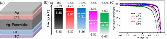
Figure 1. (a) Schematic illustration of perovskite solar cells structure. (b) Energy level diagram of Ag-incorporated perovskite film. (c) J-V performance of Ag-incorporated perovskite devices with structure of ITO/NiOx/perovskite/PCBM/Al.(Image by SINANO)
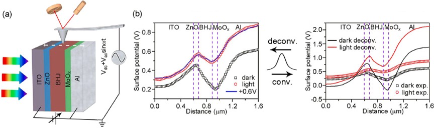
Figure 2. (a) Schematic illustration of cross-sectional SKPM imaging in operando inverted OPV devices. (b) A deconvolution protocol has been devised to recover the true energy depth profiles in operando inverted OPV devices.(Image by SINANO)
Reference:
http://www.ingentaconnect.com/content/apcs/apcs/2017/00000033/00000010/art00008
http://pubs.acs.org/doi/10.1021/acs.nanolett.7b00847
https://www.nature.com/articles/ncomms8745
http://www.sciencedirect.com/science/article/pii/S2211285517305281
Contact Information:
Prof. CHEN Liwei, Suzhou Institute of Nano-Tech and Nano-Bionics, Chinese Academy of Sciences
Email: lwchen2008@sinano.ac.cn


