Recently, a research team led by Prof. An Dingsun in Vacuum Interconnected Nanotech Workstation (Nano-X), Suzhou Institute of Nano-Tech and Nano-Bionics (SINANO), Chinese Academy of Sciences (CAS) has reported the realization of surface band bending on Ga-polar n-GaN and ion sputter induced interfacial reaction in prototypical metal-GaN system by XPS studies.
Surface pretreatments on GaN before metal deposition, such as reactive ion etching and inductively coupled plasma etching, have been found to be able to reduce the resistivity of metal/n-GaN contacts effectively. Surface N-vacancies on n-GaN are usually considered to be benefit to achieving low contact resistivity. Other surface states, such as oxides and absorbates, may have comparable effects on the contact resistivity too, but have been seldom investigated so far.
Surface band bending is a measure of internal compensation states in space charge region and thus the surface states (the denser the internal compensation states are, the less the compensation from surface states will be). Angular dependent X-ray photoelectron spectroscopy (ADXPS) was used to detect photoelectrons emitted from different depth of sample, and thus to characterize surface band bending. In this work, core level on surface was determined by collecting photoelectrons emitted within the detection depth of first several monolayers, and core level in bulk was estimated to the best by collecting photoelectrons with the deepest emission depth.
We have observed the surface band bending of GaN that induced with different surface treatments, which were calculated to be 0.84±0.21 eV, 1.24±0.21 eV, and 0.47±0.21 eV on as-grown, cleaned, and ICP etched GaN surface, respectively. We have also figured out the origins of the surface band bending by taking surface states into the analysis. A close correlation between oxygen-containing absorbates (besides N-vacancies) and surface band bending has been established: lower the surface O-H content is, smaller the shift in binding energy. This work provide helpful insights to understand physical mechanism of Ohmic contact of n-GaN (lower surface band bending usually leads to lower barrier height) and further to guide device fabrication.
On the other hand, there have been extensive researches on ion-sputter depth profiles of metal/GaN systems to explore the contact properties, however, interfacial reactions induced by ion-sputter were seldom studied in depth and details. Here, we applied in-situ XPS profile to analyze the ion sputtered surfaces. Interestingly, we found that ion sputter induced the formation of metallic Ga layer and TiCx compounds at the metal/GaN interface.
These ion-sputter-induced interfacial reactions and products alter the chemical states and compositions on GaN surface, which could be characterized by the corresponding core level peak intensity and binding energy. This phenomenon must be considered with caution either for data analysis of depth profiling or properly understanding of the contact properties.
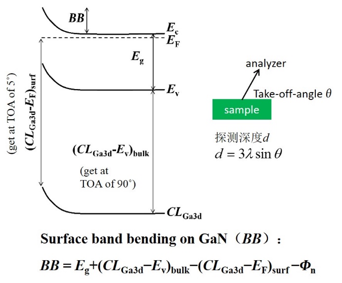
Figure.1 Schematic diagram of surface band bending on n-GaN.(Image by SINANO)
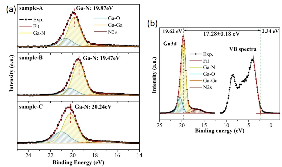
Figure. 2 (a) Ga 3d core levels of n-GaN after different surface treatments (measured at TOA of 5?); (b) Ga 3d core level and valence band (VB) spectra of sample-B cleaned with alkaline (measured at TOA of 90?).(Image by SINANO)
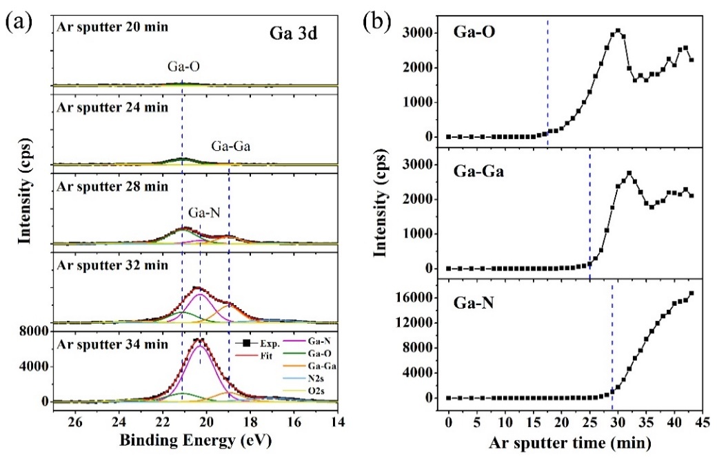
Figure. 3 Ga element variation with ion depth profile of Pd (10 nm) / Ti (10 nm) / GaN. (a) A serial of Ga 3d core level spectra during sputtering with binding energy in the range of 14-27 eV. After subtracting the Shirley background, the Ga 3d peak could be de-convoluted into five peaks. (b) Depth profile of different Ga components (Ga-O, Ga-Ga and Ga-N) calcuated from Ga 3d peak as function of sputter time.(Image by SINANO)
Contact information: Prof. An Dingsun, Suzhou institute of Nano-Tech and Nano-Bionic, Chinese Academy of Sciences.
Email: adingsun2014@sinano.ac.cn
Reference: https://doi.org/10.1016/j.apsusc.2018.01.196
https://www.nature.com/articles/s41598-018-26734-5


