Optoelectronic devices such as organic light emitting and photovoltaic are evolving towards large area, lightness, low cost, flexibility and stretchability. The demand for high-performance flexible and stretchable transparent conductive films (TCFs) is growing rapidly. At present, the widely used transparent conductive material is ITO, but its brittleness limits its application for flexible devices. Many alternatives to ITO have been developed, such as conductive polymer, carbon materials and metallic nanowires. The metal-mesh approach has come out as a winner due to its high conductivity and optical transmittance, as well as flexibility.
The conventional technology for making metal-mesh TCFs relays on complicated lithography and etching processes, which is costly and environmental unfriendly. The Printable Electronics Research Center (PERC) at Suzhou Institute of Nanotech and Nanobionics (SINANO), Chinese Academy of Sciences (CAS), developed a novel hybrid printing technology a few years ago. It is the combination of imprinting and nanosilver ink printing, which can produce embedded metal-mesh with sheet resistance below 10 Ω/□ and optical transmittance above 88%. The technology has been implemented in large scale manufacturing at O-film and the mass produced metal-mesh TCFs have been integrated in touch panels and commercialized.
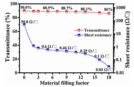
Recently, the research group led by Prof. SU Wenming of PERC has made a breakthrough to improve the conductivity of embedded metal mesh TCF. High aspect ratio embedded Cu metal-mesh was achieved by introducing an additional electroplating of Cu. Metallic Cu mesh lines with 2:1 depth to width ratio of imprinted grooves are completely filled with copper and the minimum linewidth is 4 μm. The Cu metal-mesh has extremely low sheet resistance (RS) down to 0.03 Ω □-1 and still maintains optical transmittance of 86% as shown in the figure, which translates into the figure of merit (FOM) more than 8 × 10⁴, the highest of all reported transparent conductive films.

Figure 1. Sheet resistance and the average optical transmittance versus material filling factor.(Image by SINANO)
This work has been published in Advanced Electronic Materials (DOI: 10.1002/aelm.201800991), entitled “Printable High-Aspect Ratio and High-Resolution Cu Grid Flexible Transparent Conductive Film with Figure of Merit over 80 000”, and it was financially supported by National Program on Key Research Project, National Natural Science Foundation of China, Program on Key Research Project of Jiangsu Province of China and National Science Foundation of China.
Contact Information:
Prof. Su Wenming, Printable Electronics Research Center, Suzhou institute of Nano-Tech and Nano-Bionic, Chinese Academy of Sciences
Email: wmsu2008@sinano.ac.cn
Reference:
https://onlinelibrary.wiley.com/doi/pdf/10.1002/aelm.201800991

