Recently, monolithic integration of AlGaN/GaN high-electron mobility transistors (HEMTs) with GaN-based gate drivers has attracted considerable attention for power converter systems. Complementary metal oxide semiconductor (CMOS), main inverters developed for GaN-based gate drivers, is combined with an E-mode HEMT and an E-mode p-channel HFET, which offers the lower power consumption in comparison to GaN-based DCFL.
E-mode operation is strongly desired for safe operations of power switching systems. However, several approaches to achieving E-mode suffer from a trade-off between the ON/OFF ratio, the ON-state current (|ION|) and the threshold voltage (VTH).
Recently, prof. ZHANG Baoshun’s team from Suzhou Institute of Nano-tech and Nano-bionics (SINANO) of the Chinese Academy of Sciences proposed a modified p-channel device structure by introducing an n-GaN cap layer between the GaN channel layer and the gate metal. The simulations are performed to demonstrate the possibility to break the limitations between the ON/OFF ratio, |ION| and VTH. The related research results were published in Applied Physics Letter.
For the p-channel devices, introducing a base contact or a recessed gate to the 2DEG are effective ways to achieve E-mode operation, but severe degradation in |ION| was observed when the HFET changes from D-mode to E-mode.
While in the modified HFETs, the n-GaN cap is applied as an additional measure in modulating the density of 2DHG. A combination of the n-GaN cap and the 2DHG in the gate region acts like a PN diode and subsequently a depletion region is mainly formed in the GaN channel under the gate. An improvement in Vth from 0.4V to -1.95V is achieved by thinning the GaN channel layer. Meantime, the |ION| of the device with thin GaN channel is reduced by only 1.4% compared to that with thick channel. The density of 2DHG outside the gate remained unaffected, thus not increasing the source-to-drain resistance. Furthermore, E-mode operation can also be achieved by increasing n-GaN doping concentration (Ncap) and the |ION| and ON/OFF ratio remain almost unchanged with respect to Ncap.
The structure proposed can be grown with the current deposition techniques, which will guide to the scientific groups that are working on the growth and fabrication of HFET transistors.
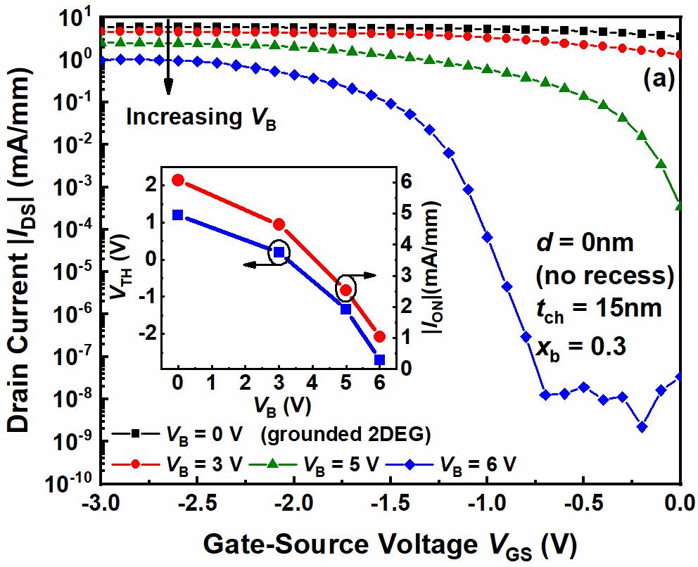
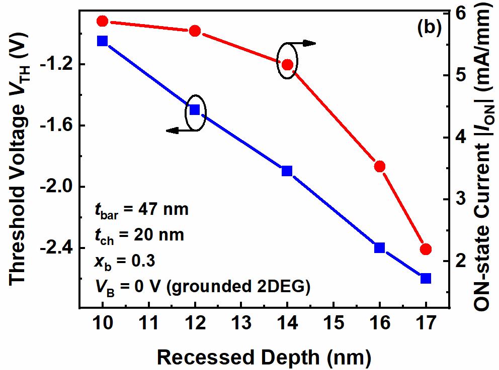
Figure 1. (a) Simulated transfer characteristics at various base to source bias (VB) in the conventional HFETs. (b) Comparison of the threshold voltage |VTH| and |ION| vs. recess etch depth d. The inset in (a) exhibits the corresponding VTH and |ION| behavior with respect to VB.
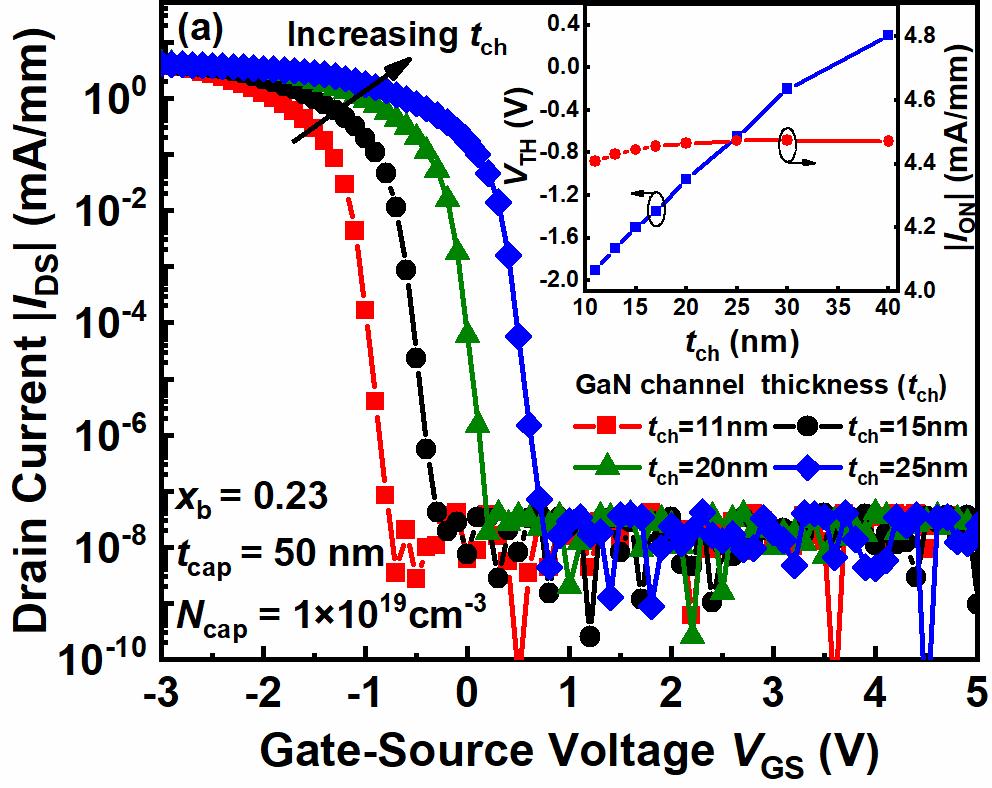
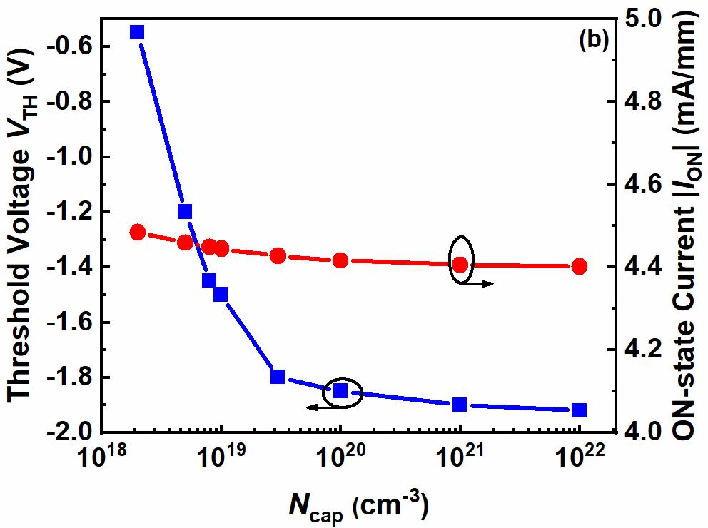
Figure 2. (a) Comparison of the simulated transfer characteristics with a variation in the GaN channel thickness tch. (b) The change in VTH and |ION| owing to different n-GaN doping concentration Ncap.
Contact information: Prof. ZHANG Baoshun,Suzhou Institute of Nano-Tech and Nano-Bionics, Chinese Academy of Sciences.
Email:bszhang2006@sinano.ac.cn
Reference:https://www.osapublishing.org/ol/abstract.cfm?uri=ol-44-18-4562


