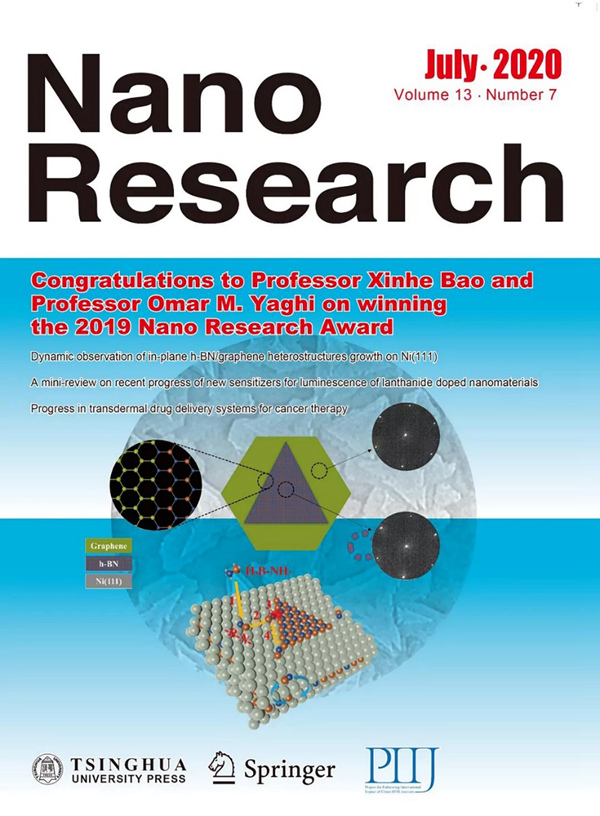
In-plane two-dimensional heterostructures efficiently integrate the advantages of different two-dimensional materials and expand their applications in optical and electrical devices. However, the controllable and large-scale synthesis of epitaxial heterostructures, especially the micro-mechanism of the fabricated process remains to be further studied. Prof. Xinhe Bao and prof. Yi Cui have directly epitaxially grown in-plane hexagonal boron nitride (h-BN)/graphene heterostructures on Ni (111) surfaces by chemical vapor deposition (CVD), in situ monitoring by the dynamic imaging. And the effect of h-BN as a nucleation template on the construction of epitaxial heterostructures was systematically studied. It has been found that when the growth order of h-BN is prior to that of graphene, the graphene epitaxially grows along the h-BN edges and forms epitaxial structure, resulting in the single oriented epitaxial heterostructures. When graphene firstly nucleates, the graphene/Ni(111) interface interaction is weakened by near-surface carbon species in the substrate, leading to non-epitaxial growth. Following these non-epitaxy templates, the h-BN also grows as the non-epitaxial way, in which the high-quality two-dimensional heterostructures is expected to be hardly obtained. In addition, this work has revealed that the growth mechanism of h-BN on Ni (111) surface follows diffusion-limited aggregation (DLA) rather than reaction-limited aggregation (RLA). The findings provide insights into the synthesis of well-defined h-BN/graphene heterostructures and deep understanding of the growth dynamics of h-BN on metal surfaces. This study named “Dynamic observation of in-plane h-BN/graphene heterostructures growth on Ni(111)” has been published on Nano Research (Nano Research (2020):1-6) as a front cover. Introduction to Nano-X The work was performed in the Vacuum Interconnected Nanotech Workstation (NANO-X) of Suzhou Institute of Nano-Tech and Nano-Bionics, the Chinese Academy of Science. NANO-X is currently the largest vacuum interconnected facility including material preparation, performance test, and device technology in the world, which is promising to be built into a world-leading scientific user facility in the future. In this system, the instruments for surface-interface analysis are interconnected by ultrahigh vacuum (UHV) tubes where samples can be transferred from one endstation to another one, avoiding the dirty from the atmosphere. It can be clarified into the following sections: Characterization in extreme conditions (ULT-STM, 4P-STM); Testing in controllable atmosphere (NAP-STM; NAP-XPS, SNOM); Surface and interface spectroscopy (XPS/UPS, TOF-SIMS); surface and interface imaging (XPS-mapping, SEM, PEEM, LEEM, STM, SNOM, SIMS-mapping); Optical Analysis (Raman, PL). The platform can meet the following requirements: (1) Characterization of surface morphology and composition of materials at multi-scale (from atomic scale to mesoscopic scale) ; (2) Analysis of element distribution and chemical state in multi-dimension (from two dimension to three dimension) ; (3) Dynamic detection of gas/solid interface in near-ambient pressure environment; (4) Test of device performance under limit conditions.  |

